Wednesday, October 15, 2014
Browse »
home »
a
»
build
»
circuit
»
diagram
»
digital
»
Theremin
»
Build a Digital Theremin Circuit Diagram
Digital Theremin Circuit Diagram
Build a Digital Theremin Circuit Diagram
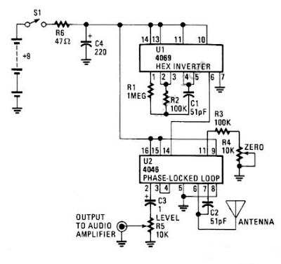
Theremin circuit shown in this schematic diagram uses digital component, so we can call it a digital Theremin. This circuit employs logic inverter 74C04 or CD4069 hex inverter and CD4046 phase-locked-loop (PLL) IC.
The CD4069 logic inverter is operated as a fixed-frequency oscillator with frequency around 100kHz. The CD4046 is operated as a variable frequency oscillator which is adjustable around 100kHz. The exact center frequency of the on-chip oscillator is determined by R4, C2 and R3. Here is the schematic diagram of the circuit.
Digital Theremin Circuit Diagram
The frequency of variable oscillator frequency circuit can be shifted several kilohertz by moving your hand approaching the antenna since the C2 and the antenna form an equivalent parallel capacitance. The frequency of the variable oscillator should be set to the same frequency of fixed oscillator when there is no hand or human body close to the antenna.
This calibration is done by adjusting the zero control R4 pot with this simple rule: If both oscillators (the fixed and the variable) are set to the same frequency then the Theremin will produce no output (silent). This Theremin circuit will start producing audible tone if you move your hand approaching the antenna since it will shift the frequency of the variable oscillator. You can play this Theremin circuit by moving your right hand around the antenna and at the same time turning the volume knob R5 with your left hand.
Subscribe to:
Post Comments (Atom)

No comments:
Post a Comment