Wednesday, November 5, 2014
Portable Microphone Preamplifier
This circuit is mainly intended to provide common home stereo amplifiers with a microphone input. The battery supply is a good compromise: in this manner the input circuit is free from mains low frequency hum pick-up and connection to the amplifier is more simple, due to the absence of mains cable and power supply. Using a stereo microphone the circuit must be doubled. In this case, two separate level controls are better than a dual-ganged stereo potentiometer. Low current drawing (about 2mA) ensures a long battery life.
Circuit Operation:
The circuit is based on a low noise, high gain two stage PNP and NPN transistor amplifier, using DC negative feedback through R6 to stabilize the working conditions quite precisely. Output level is attenuated by P1 but, at the same time, the stage gain is lowered due to the increased value of R5. This unusual connection of P1, helps in obtaining a high headroom input, allowing to cope with a wide range of input sources (0.2 to 200mV RMS for 1V RMS output).
Portable Microphone Preamplifier Circuit diagram:
P1 = 2.2K
R1 = 100K
R2 = 100K
R3 = 100K
R4 = 8.2K
R5 = 68R
R6 = 6.8K
R7 = 1K
R8 = 1K
R9 = 150R
C1 = 1uF-63V
C2 = 100uF-25V
C3 = 100uF-25V
C4 = 100uF-25V
C5 = 22uF-25V
Q1 = BC560
Q2 = BC550
Notes:
- Harmonic distortion is about 0.1% @ 1V RMS output (all frequencies).
- Maximum input voltage (level control cursor set at maximum) = 25mV RMS
- Maximum input voltage (level control cursor set at center position) = 200mV RMS
- Enclosing the circuit in a metal case is highly recommended.
- Simply connect the output of this device to the Aux input of your amplifier through screened cable and suitable connectors.
4 X 15 Watt Mini Power Amplifier
A lot of electronic circuits in the domain of audio amplifiers are already been published here. This circuit is a little different because it is a four channel amplifier. Each channel of this amplifier can deliver an output of 15Watts into a 4 ohm speaker. The amplifier can be operated from a single 12V DC supply and this makes it possible to use this amplifier in car audio applications too.
4 X 15 Watt Mini Power Amplifier Circuit Diagram :
![4X15W-amplifier-circuit]()
The circuit is based on the 15W BTL X 2 channel audio power amplifier IC TA8215 from Toshiba. Even though chip is specifically designed for car audio applications it can be also used for home audio applications. Two TA8215 ICs are used here in order to obtain a 4 channel amplifier system. The circuit is designed almost exactly as per the application diagram in the ICs datasheet. Pins 7 and 19 are the Vcc pins of the ICs internal integrated power amplifier stages and these pins are connected to the positive supply. Pin 9 is the Vcc pin for ICs internal preamplifier and it is also connected to the positive supply. Pins 13 and 14 are the internal power amplifiers ground pins and they are tied together and connected to the ground.
The internal preamplifier’s ground pin (pin5) is connected to the common ground through a 10 Ohm resistor which makes the input ground separated from the common ground by a resistance of 10 ohms and this improves the noise rejection. The 100uF capacitor works as a power supply de-coupler. The resistor networks connected to the output lines of each amplifier improves the high frequency stability. The variable resistors (R3, R4, R12 and R13) works as the volume controller for the corresponding channels.
Notes :
4 X 15 Watt Mini Power Amplifier Circuit Diagram :
The internal preamplifier’s ground pin (pin5) is connected to the common ground through a 10 Ohm resistor which makes the input ground separated from the common ground by a resistance of 10 ohms and this improves the noise rejection. The 100uF capacitor works as a power supply de-coupler. The resistor networks connected to the output lines of each amplifier improves the high frequency stability. The variable resistors (R3, R4, R12 and R13) works as the volume controller for the corresponding channels.
Notes :
- Assembling the circuit on a good quality PCB is a must for obtaining optimum sound quality.
- Use 12V DC for powering the circuit.
- The ICs must be fitted with adequately sized heat sinks.
- R3, R4, R12 and R13 serves as volume controllers.
- K1 to K4 can be 4 Ohm, 20W speakers.
- This amplifier circuit can be used in a variety of applications such as car audio systems, home theater systems, personal audio systems, public address systems etc.
Tuesday, November 4, 2014
Stereo Power Amplifier Circuit based on BA5417
BA5417 is a stereo amplifier IC with a lot of good features like thermal shut down, standby function, soft clipping, wide operating voltage range etc. The IC can deliver 5W per channel into 4 ohm loud speakers at 12V DC supply voltage. The BA5417 has excellent sound quality and low THD (total harmonic distortion) around 0.1% at F=1kHz; Pout=0.5W.
Stereo Power Amplifier Circuit diagram :
Setup and working of this stereo power amplifier circuit is somewhat similar to the BA5406 based stereo amplifier circuit published previously. C10 and C11 are DC decoupling capacitors which block any DC level present in the input signals. C2 and C6 couples the amplifiers left and right power outputs to the corresponding loud speakers. C1 and C5 are bootstrap capacitors.
Bootstrapping is a method in which a portion of the amplifiers is taken and applied to the input. The prime objective of bootstrapping is to improve the input impedance. Networks R1,C3 and R2,C7 are meant for improving the high frequency stability of the circuit. C4 is the power supply filter capacitor. S1 is the standby switch. C8 is a filter capacitor. R3 and R4 sets the gain of the left and right channels of the amplifier in conjunction with the 39K internal feedback resistors.
Note :
- Supply voltage range of BA5417 is from 6 to 15V DC.
- The recommended supply voltage for this circuit is 12V DC.
- The power supply must be well regulated and filtered.
- BA5417 requires a heatsink.
- The circuit can be assembled on a perf board without much degradation in performance.
UHF antenna booster circuit diagram
UHF Antenna BoosterUHF antenna booster can be used for better reception, especially when you’re far from TV station / relay transmitter. This UHF antenna booster works in 400-850 MHz range. Here is the circuit diagram of the UHF antenna booster: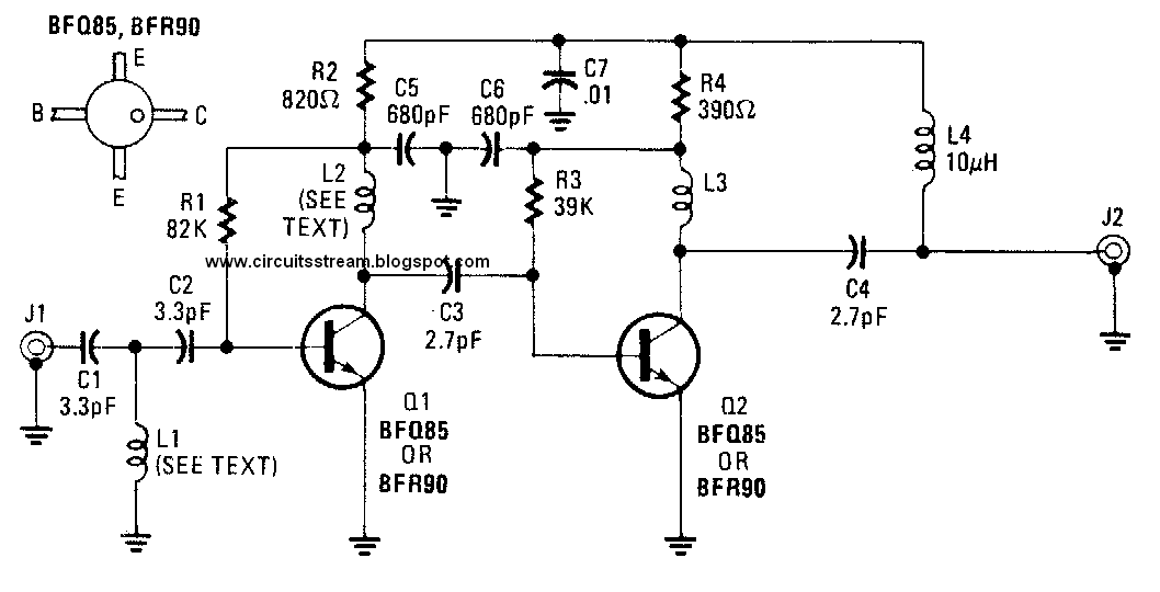
Read More..
The circuit use only one transistor, but it gives you 10 to 15 dB amplification, enough for many situation. The most important part is that the transistor circuitry should be shielded from the input circuitry, as shown in the schematic diagram by the dashed line. This ircuit is powered via the signal cable, since the antenna booster circuit must be wired as close as possible to the antenna. This is very important since the amplifier should amplify the signal acquired by the antenna, not the noise picked by the cable from the antenna to the circuit. The antenna and the booster circuit can be installed above your house’s roof. Long 75 ohm coaxial cable can be drawn from the this booster circuit output to the power supply unit close to TV set.
Just insert a 50-10o uH inductor or RF choke between the output cable and the power supply. Tap the output signal from the output cable using a small 100pF ceramic capacitor to block the DC voltage from the power supply. Adjust P1 to get the best reception, and this should set the working current consumption to around 5-15 mA.
Monday, November 3, 2014
Versatile Micropower Battery Protector
Protect your expensive batteries from discharge damage with this mini-sized electronic cutout switch. It uses virtually no power and can be built to suit a wide range of battery voltages.
Main Features

![versatile-micropower-battery-protector-circuit-backside]()
Back in May 2002, we (Silicon Chip) presented the "Battery Guardian", a project designed specifically for protecting 12V car batteries from over-discharge. This unit has proven to be very popular and is still available from kit suppliers. This new design does not supersede the Battery Guardian – at least not when it comes to 12V car batteries. Instead, it’s a more flexible alternative that can be used with a wide range of battery voltages.
Parts layout:
![front-parts-layout-versatile-micropower-battery-protector-circuit]()
![back-parts-layout-versatile-micropower-battery-protector-circuit]()
In this new "Micropower Battery Protector", we’ve dispensed with the low-battery warning circuitry and the relatively cheap N-channel MOSFET used in the Battery Guardian in favour of a physically smaller module that steals much less battery power. It costs a little more but can switch lower voltages, allowing it to be used with 6V & 12V lead-acid batteries and 4-cell to 10-cell NiCd and NiMH battery packs.
![pcb-layout-versatile-micropower-battery-protector-circuit]()
Most battery-powered equipment provides no mechanism for disconnecting the batteries when they’re exhausted. Even when the voltage drops too low for normal operation, battery drain usually continues until all available energy is expended. This is particularly true of equipment designed to be powered from alkaline or carbon cells but retro-fitted with rechargeables.
Circuit diagram:
![versatile-micropower-battery-protector-circuit-diagram]()
Another example is emergency lighting and security equipment designed to be float-charged from the mains. In an extended blackout period, the batteries can be completely drained and may not recover when the mains power is finally restored.
Main Features
- Disconnects load at preset battery voltage
- Automatically reconnects load when battery recharged
- Ultra-low power consumption (<20ma)
- Miniature size
- 10A maximum rating
- Suitable for use with 4.8-12.5V batteries
- Transient voltage protection (optional)
- Cars, boats & caravans
- Security systems
- Emergency lighting
- Small solar installations
- Camera battery packs
- Many other low-power applications
Back in May 2002, we (Silicon Chip) presented the "Battery Guardian", a project designed specifically for protecting 12V car batteries from over-discharge. This unit has proven to be very popular and is still available from kit suppliers. This new design does not supersede the Battery Guardian – at least not when it comes to 12V car batteries. Instead, it’s a more flexible alternative that can be used with a wide range of battery voltages.
In this new "Micropower Battery Protector", we’ve dispensed with the low-battery warning circuitry and the relatively cheap N-channel MOSFET used in the Battery Guardian in favour of a physically smaller module that steals much less battery power. It costs a little more but can switch lower voltages, allowing it to be used with 6V & 12V lead-acid batteries and 4-cell to 10-cell NiCd and NiMH battery packs.
PCB layout:
Most battery-powered equipment provides no mechanism for disconnecting the batteries when they’re exhausted. Even when the voltage drops too low for normal operation, battery drain usually continues until all available energy is expended. This is particularly true of equipment designed to be powered from alkaline or carbon cells but retro-fitted with rechargeables.
Circuit diagram:
Another example is emergency lighting and security equipment designed to be float-charged from the mains. In an extended blackout period, the batteries can be completely drained and may not recover when the mains power is finally restored.
FLASH LIGHT ELECTRONIC DIAGRAM

FLASH LIGHT ELECTRONIC DIAGRAM
IC NE555 works as an astable multivibrator with variation on the frequency. With this circuit, the LED blinks every half second. How long the blink time is, can be adjusted by adjusting the value of capacitor C1. Up to 18 additional LEDs can be attached to this circuit (36 LEDs total).
Components :
Diode D1-D2 : 5mm LED
Resistor R1 : 4K7 ohm
Resistor R2 : 1k ohm
Resistor R3-R4 : 330 ohm
Variable resistor VR1 : 100k ohm
Polar capacitor C1 : 10 uF/10 V
Capacitor C2 : 0.01 uF
IC1 : NE555
6V power supply
Sunday, November 2, 2014
tda4605 datasheet
tda4605
CONTROL CIRCUIT FOR SWITCH MODE POWER SUPPLIES USING MOS TRANSISTORS

The IC TDA4605controls the MOS PowerTransistor and performs all necessary regulation and
monitoring functions in free running flyback converters.
Since good load regulation over a wide load range is attained, this IC is particularly suitable
for Consumer as well asIndustrial PowerSupplies.
Alternative source of theTDA4605 is alsoavail-
ablefrom SIEMENS semiconductors Consumer ElectronicsA.G.
IRF740 Datasheet power MOSFET
N - CHANNEL 400V - 0.48 Ω - 10 A - TO-220
PowerMESH MOSFET
This power MOSFET is designed using the company’s consolidated strip layout-based MESH OVERLAY process. This technology matches and improves the performances compared with standard parts from various sources.
APPLICATIONS
# HIGH CURRENT SWITCHING
# UNINTERRUPTIBLE POWER SUPPLY (UPS
# DC/DC COVERTERS FOR TELECOM,
# INDUSTRIAL, AND LIGHTING EQUIPMENT

MOSFET, N, 400V, 10A, TO-220; Transistor Type:MOSFET; Transistor Polarity:N; Voltage, Vds Typ:400V; Current, Id Cont:10A; Resistance, Rds On:0.55ohm; Voltage, Vgs Rds on Measurement:10V; Voltage, Vgs th Typ:4V; Case Style:TO-220AB; Termination Type:Through Hole; Current, Idm Pulse:40A; Power Dissipation:125W; Power, Pd:125W; Thermal Resistance, Junction to Case A:1 C/W; Voltage, Vds Max:400V
Read More..
PowerMESH MOSFET
This power MOSFET is designed using the company’s consolidated strip layout-based MESH OVERLAY process. This technology matches and improves the performances compared with standard parts from various sources.
APPLICATIONS
# HIGH CURRENT SWITCHING
# UNINTERRUPTIBLE POWER SUPPLY (UPS
# DC/DC COVERTERS FOR TELECOM,
# INDUSTRIAL, AND LIGHTING EQUIPMENT
MOSFET, N, 400V, 10A, TO-220; Transistor Type:MOSFET; Transistor Polarity:N; Voltage, Vds Typ:400V; Current, Id Cont:10A; Resistance, Rds On:0.55ohm; Voltage, Vgs Rds on Measurement:10V; Voltage, Vgs th Typ:4V; Case Style:TO-220AB; Termination Type:Through Hole; Current, Idm Pulse:40A; Power Dissipation:125W; Power, Pd:125W; Thermal Resistance, Junction to Case A:1 C/W; Voltage, Vds Max:400V
Saturday, November 1, 2014
9V Battery Replacement Power Supply Circuit Diagram
This circuit was originally designed to power a motorcycle intercom from the vehicle supply system. This type of intercom, which is used for communication between driver and passenger, generally requires quite a bit of power. In order to improve intelligibility there is often elaborate filtering and a compander is sometimes used as well. The disadvantage is that a battery doesn’t last very long. You could use rechargeable batteries, of course, but that is often rather laborious. It seems much more obvious to use the motorcycle power supply instead. A 9-V converter for such an application has to meet a few special requirements.
9V Battery Replacement Power Supply Circuit Diagram
![9V]()
9V Battery Replacement Power Supply Circuit Diagram
For one, it has to prevent interference from, for example, the ignition system reaching the attached circuit. It is also preferable that the entire circuit fits in the 9-V battery compartment. This circuit meets these requirements quite successfully and the design has nonetheless remained fairly simple. In the schematic we can recognize a filter, followed by a voltage regulator and a voltage indicator. D1, which protects the circuit against reverse polarity, is followed by an LC and an RC filter (C3/L1/L2/C1/R1/C2). This filter excludes various disturbances from the motorcycle power system.
Moreover, the design with the 78L08 and D3 ensures that the voltage regulator is operating in the linear region. The nominal system voltage of 14 V can sometimes sag to about 12 V when heavy loads such as the lights are switched on. Although the circuit is obviously suitable for all kinds of applications, we would like to mention that it has been extensively tested on a Yamaha TRX850. These tests show that the converter functions very well and that the interference suppression is excellent.
Friday, October 31, 2014
Stun Gun Circuit Diagram
This gadget generates substantial voltage pulses which can disrupt muscle tissues and neurological system, forcing any individual who touches it in a condition of mental bewilderment. The unit may be used again attacking beasts or dangerous intruders. Be aware that, this gadget could be prohibited in your country. It may be extremely dangerous for folks with cardiac issues, who may be using external electronic apparatus (like peacemakers), since it can deliver quite a little RF. Dont attempt reckless behavior using this gadget, it is far from a plaything.
The proposed stun gun circuit description may be understood as follows:
The 555 IC is connected as a astable to generate rectangular waves with variable frequency and duty cycle (see the potentiometers and diode). This signal is fed to a IRF840 Mosfet (not necessary to incorporate totem transistor network, as frequency would be reduced, nonetheless the IC has adequate current potential to swiftly charge/discharge the gate).
As an alternative for the mosfet a bipolar transistor works extremely well (add a 100 ohm resistor between 555 and base of the transistor). Proper BJT could be BU406, but additionally scaled-down BJT may be ok, take into account that it should be able to cope with a minimum of 2A nonstop.
The inductive boost snubber isnt called for since the electrical power is lower which is practically completely adsorbed to charge the tank capacitor, furthermore because this gadget is battery powered we dont wish to disperse the power on a resistor, yet we need to produce the sparks.
With a snubbing system you are going to encounter decreased firing levels. Utilize A PUSHBUTTON SWITCH FOR Protection
Building the Transformer: this could be the actual tedious aspect. Because it in retailers we have to construct these. Components essential: enamel copper wire (0.20 mm or 0.125 mm), ferrite rod, LDPE sheets (0.25 mm).
Coat the ferrite rod with a application of ldpe (polyethylene, as a substitute utilize electric insulating tape) and stick it (or tape it) Position 200-250 winding on the ldpe (a lot more winding would do in case the rod is more than 1), an additional ldpe application, yet another 200-250 winding and so forth to eventually have 5-6 tiers (approx 1000-1400 turns nonetheless supplementary turns wouldnt negatively affect the functionality), then again be cautious for internal arcing that could destroy it.
Insulate it once more and set the primary winding, 15-20 turns of 1mm wire would be simply fine, an excessive amount of winding will probably lead to lesser current and reduced spike in T2 secondary on account of decreased rise period, and too few is not going to saturate the core.
Go for MKP capacitors since they have minimal ESR and ESL (these are popular in tesla coils as mmc capacitors).
The spark opening could be straightforwardly a pair of crossed (although not touching) 1 mm spaced wires. It works like a voltage regulated switch, firing when the voltage is just nice to ionize the air between them (transforming it to plasma with smaller resistance). Remember that it could be sensible do put it into a compact plastic box and stuff with oil allowing bubbles away dont employ motor oil or frying oil, rather organic mineral oil which includes zero water inside.
Stun Gun Circuit Diagram
![Simple]()
Simple Stun Gun Circuit Diagram
Model Railway Short Circuit Beeper
Short circuits in the tracks, points or wiring are almost inevitable when building or operating a model railway. Although transformers for model systems must be protected against short circuits by built-in bimetallic switches, the response time of such switches is so long that is not possible to immediately localise a short that occurs while the trains are running, for example. Furthermore, bimetallic protection switches do not always work properly when the voltage applied to the track circuit is relatively low.
Model Railway Short-Circuit Beeper Circuit diagram :
Model Railway Short-Circuit Beeper Circuit Diagram
The rapid-acting acoustic short-circuit detector described here eliminates these problems. However, it requires its own power source, which is implemented here in the form of a GoldCap storage capacitor with a capacity of 0.1 to 1 F. A commonly available reed switch (filled with an inert gas) is used for the current sensor, but in this case it is actuated by a solenoid instead of a permanent magnet. An adequate coil is provided by several turns of 0.8–1 mm enamelled copper wire wound around a drill bit or yarn spool and then slipped over the glass tube of the reed switch. This technique generates only a negligible voltage drop. The actuation sensitivity of the switch (expressed in ampèreturns or A-t)) deter-mines the number of turns required for the coil. For instance, if you select a type rated at 20–40 A-t and assume a maxi-mum allowable operating current of 6 A, seven turns (40 ÷ 6 = 6.67) will be sufficient. As a rule, the optimum number of windings must be determined empirically, due to a lack of specification data.
As you can see from the circuit diagram, the short-circuit detector is equally suitable for AC and DC railways. With Märklin transformers (HO and I), the track and lighting circuits can be sensed together, since both circuits are powered from a single secondary winding.
Coil L1 is located in the common ground lead (‘O’ terminal), so the piezoelectric buzzer will sound if a short circuit is present in either of the two circuits. The (positive) trigger voltage is taken from the lighting circuit (L) via D1 and series resistor R1. Even though the current flowing through winding L1 is an AC or pulsating DC current, which causes the contact reeds to vibrate in synchronisation with the mains frequency, the buzzer will be activated because a brief positive pulse is all that is required to trigger thyristor Th1. The thyristor takes its anode voltage from the GoldCap storage capacitor (C2), which is charged via C2 and R2. The alarm can be manually switched off using switch S1, since although the thyris-tor will return to the blocking state after C2 has been discharged if a short circuit is present the lighting circuit, this will not happen if there is a short circuit in the track circuit. C1 eliminates any noise pulses that may be generated.
As a continuous tone does not attract as much attention as an intermittent beep, an intermittent piezoelectric generator is preferable. As almost no current flows during the intervals between beeps and the hold current through the thyristor must be kept above 3 mA, a resistor with a value of 1.5–1.8 kΩ is connected in parallel with the buzzer. This may also be necessary with certain types of continuous-tone buzzers if the operating current is less than 3 mA. The Zener diode must limit the operating voltage to 5.1 V, since the rated volt-age of the GoldCap capacitor is 5.5 V.
Thursday, October 30, 2014
20A Transformerless Power Supply
| 20A Transformerless Power Supply |
This PSU has been abnormally advised in place of current-hungry ham telephone system transceivers. It delivers vigilantly in relation to 20Amps on 13.8V. For cut currents, a distant received attached output, able of 15ma up to a absolute of 20A has been added. accede to us ensure what did you say? we consent got at this time. The skill agent must remain able to bear by atomic 25A at 17.5 to 20V. The reduce the voltage, the lower power dissipation. The rectified conventional willpower be �ironed� by the C1, whose accommodation ought to not be beneath than 40.000uF, (a aureate adage of nearly 2000uF/A), but we give enthusiastic approval to up to 50.000uF. This accommodation can subsist present at birth up by several abate capacitors inside congruence. The wretched of this architecture is a trouble-free 12V supervisor (7812). The achievement voltage can be brought to adapted amount (now 13.8V) by two alien resistors (R5 and R6) claim this formula:
U= 12(1+R5/R6)
The low currents (at this time 15mA) self-control accumulate the 7812 in its permitted function. for instance shortly as the customary rises greater than 15ma, the voltage bead on R4 will amenable the Q3, certainly administration the aerial achievement current. This is a PNP transistor (Ic>25) and established addition agency of next to atomic 20. The lone with the intention of has been activated and accurate reality is the 2N5683. The acknowledged attached attrition RL, in support of the superlative achievement of 20 Amps be supposed to take place 0.03 Ohms, rated by
slightest 15W. You can help the attrition wire or else in relation to-cope with several resistors clothed in comparable, increase the resistance/power ideals. Ethics used for added currents can be affected by the government:
RL=0.7/Imax
The RL and Q2 (3A PNP such in the same way as BD330) anatomy a abbreviate ambit automatic fuse. As in a bit as the preeminent usual alcove 20Amps, the voltage bead in excess of the resistor RL wish simple Q2, and appropriately absolute the B-E time-honored of Q3. Alongside to Q2 is Q1, which light the LED 1 when the accepted attached ambit is dynamic. what time the �fuse� is active, the Q2 bridges the R3, so the wealthy normal would breeze through the IC1, and accident it. Therefore the R4 is inserted, being to absolute the IC1 accepted to 15mA. This makes it understandable to run the IC1 afterwards one cooling aid. The LED 2 force alight up all spell the PSU is switched on.
in attendance is an modifiable normal limiter popular alongside to the anchored output, appropriately accouterment regulating accepted precursor on behalf of abate currents.
This ambit is authentic down-to-earth too. You desire apprehension to in attendance is refusal acknowledged analysis resistor. But it is totally here, in a anatomy of the Rds-on attrition of the N-channel FET, which absolutely handles the amount blow from the source. The exploit of the FET is perceptible featuring in the diagram 2. as the established Id is rising, the astriction Uds on top of the attrition Rds rises definite boring in the commencement, but actual fast afterwards the knick. This agency, to afore the knick the FET behaves what a resistor but afterwards it, facility as connected acknowledged source.
The D2, R3 and B-E connection of the Q4 desire faculty the Uds voltage of the FET1. what time the voltage rises sufficient, the Q4 will adjustment the FET1 aboideau to majority, and scratch the expected breeze through the FET 1 rotten. However, to sanction the FET1 to sincere, in attendance is assertive aboideau voltage crucial, which during this occurrence is brought up by the voltage link consisting of R8, Z1, P1 and R9. So the finest Aboideau voltage desire ensue the single of the Z1, and the basal will be something like 3V6. The Z1 voltage (Uz1) will appropriately actuate the do well standard affluent through the FET 1.
The diagram 2 will outer shell to facilitate pro 5 Amps the Uz1 ought to come to pass 5V6, and for 20Amps about 9V6. The Capacitor C4 desire actuate the velocity otherwise the acknowledgment point of the limiter. 100 uF will accomplish the acknowledgment time to be nearly 100ms, and 1n will accomplish it 1us.
inside the advised limits, the P1 resolve absolute the customary achievement at home the ambit of 15mA to 20A. You can handle both achievement concurrently, but the absolute achievement time-honored will come to pass bound by the amount of the RL. This PSU can be habitual additionally in lieu of college outputs, while continued as the agent yearn for lever the standard food, and you accommodate acceptable cooling for the Q3.
source : www.electronics-lab.com
LED Audio Level Meter Circuit
This circuit uses two quad op-amps to form an eight LED audio level meter. The op-amp used in this particular circuit is the LM324. It is a popular IC and should be available from many parts stores.
 |
| LED audio level meter schematic |
The 1K resistors in the circuit are essential so that the LEDs turn on at different audio levels. There is no reason why you cant change these resistors, although anything above 5K may cause some of the LEDs to never switch on. This circuit is easily expandable with more op-amps, and is not limited to use with the LM324. Pretty much any op-amp will work as long as you look up the pinouts and make sure everything is properly connected.
The 33K resistor on the schematic is to keep the signal input to the circuit at a low level. It is unlikely you will find a 33K resistor, so the closest you can get should do. The value of this resistor may need to be changed, so it is best you breadboard this circuit before actually constructing it on PCB. The circuit in its current form will accept line level inputs from sources such as the aux out on a Hi-Fi, all though could be easily modified to accept speaker inputs.
The audio + is connected to the main positive rail, while the audio - is used for signal input. The 50k pot can be used to vary the sensitivity of the circuit.
Wednesday, October 29, 2014
Valve Sound Converter Schematic
This is the simple Valve Sound Converter Schematic. ‘Valve sound’ is not just an anachronism: there are those who remain ardent lovers of the quality of sound produced by a valve amplifier. However, not everyone is inclined to splash out on an expensive valve output stage or complete amplifier with a comparatively low power output. Also, for all their aesthetic qualities, modern valve amplifiers burn up (in the full sense of the word!) quite a few watts even at normal listening volume, and so are not exactly environmentally harmless. This valve sound converter offers a cunning way out of this dilemma. It is a low cost unit that can be easily slipped into the audio chain at a suitable point and it only consumes a modest amount of energy.
A valve sound converter can be constructed using a common-or-garden small-signal amplifier using a readily-available triode. Compared to using a pentode, this simplifies the circuit and, thanks to its less linear characteristic, offers even more valve sound. For stereo use a double triode is ideal. Because only a low gain is required, a type ECC82 (12AU7) is a better choice than alternatives such as the ECC81 (12AT7) or ECC83 (12AX7). This also makes things easier for home brewers only used to working with semiconductors, since we can avoid any difficulties with high voltages, obscure transformers and the like:the amplifier stage uses an anode voltage of only 60 V, which is generated using a small 24 V transformer and a voltage doubler (D3, D4, C4 and C5).
Since the double triode only draws about 2mA at this voltage, a 1 VA or 2 VA transformer will do the job. To avoid ripple on the power supply and hence the generation of hum in the converter, the anode voltage is regulated using Zener diodes D1 and D2, and T1. The same goes for the heater supply: rather than using AC, here we use a DC supply, regulated by IC1. The 9 V transformer needs to be rated at at least 3 VA. As you will see, the actual amplifier circuit is shown only once. Components C1 to C3, R1 to R4, and P1 need to be duplicated for the second channel.
The inset valve symbol in the circuit diagram and the base pinout diagram show how the anode, cathode and grid of the other half of the double triode (V1.B) are connected. Construction should not present any great difficulties. Pay particular attention to screening and cable routing, and to the placing of the transformers to minimise the hum induced by their magnetic fields. Adjust P1 to set the overall gain to 1 (0 dB). The output impedance of 47 kΩ is relatively high, but should be compatible with the inputs of most power amplifiers and preamplifiers.
For a good valve sound, the operating point of the circuit should be set so that the audio output voltage is in the region of a few hundred millivolts up to around 1.5 V. If the valve sound converter is inserted between a preamplifier and the power amplifier, it should be before the volume control potentiometer as otherwise the sound will change significantly depending on the volume. As an example, no modifications are needed to an existing power amplifier if the converter is inserted between the output of a CD player and the input to the amplifier.
Author : Stefan Dellemann
GSM Remote Control Software
PC configuration software for all remote controls described in the last four issues. This application is used to set all parameters via PC, instead of using the boring and expensive SMS configuration system.
In the articles devoted to the remote GSM modules, we have repeatedly mentioned that the programming of the numbers in the list of those qualified to command the devices and the configuration of all operating parameters could be done avoiding the long and expensive procedure through SMS; in fact we made reference to an application software that could take advantage of the USB interface to connect with our modules and check the current settings or to add new configurations. Well, now is time to talk about this program, created to facilitate the task of those who must install our TDGs. This program is really useful for the gate opener where a lot of time could be spent entering from a mobile phone, via SMS, the many numbers a phone can contain and that would cost quite a lot (unless you have a special free SMS formula with your service provider).The software runs on Windows and needs relatively limited resources, in fact, the system requirements basically are:
- 30 MB of free space on your Hard Disk;
- a free USB port;
- XP/2000/Vista/7 OS Microsoft Windows – 32-bit or 64 bit.
This software allows you to set the settings for Remote Control, just connect the device via USB and the computer will immediately recognize the device since among other functions, our program automatically recognizes the remote that is connected. In practice, according to the connected device the program adapts its user interface, showing in the main dialog box only the tabs that relate to its configuration, excluding the rest.

Initial screen of the software
Boxes Com Port and Baud Rate summarize the information about the virtual open COM for the USB connection.
First of all, in the Information tab we find a summary of all the characteristics of the remote control during the configuration phase, i.e. model (TDG133. .. TDG140), firmware version and IMEI of the cell module installed.

In the menu bar there are two commands:
Exit which allows you to leave the program and Database which opens the window Phonebook, this window displays the stored phone numbers; in this window the buttons Clear List and Update List allow you to remove the directory or to update it. In the latter case, the program sends the new phonebook to the remote. Clicking on the question mark, instead, you get information about the program, i.e. release and more.
It should be noted that in the lower section of the main window, there is the indication “pending call from Master Number” in case you connect a remote control that has not stored at least one number, or in which the Easy Setup has not been performed.
In the same section, by clicking on Enable Extended LOG you access the dialog box shown on the left, in Figure 4, which contains all data received on the “COM” port of the computer you are using.
The Master Numbers section summarizes the numbers in the list (8 maximum) authorized to carry out the configuration and issue commands via SMS.

The Phone Numbers tab can be seen connecting any remote control version to the computer. Let’s now see the main window, specific for the TDG133 gate opener and the TDG134: note, in the right section, the tab Gate Opener Numbers, next to tab Master Numbers. By clicking on that tab, you access the window that summarizes the list of numbers related to the gate open control.


There, you can specify, for each phone number included in the list of master numbers, that in case of failure it has to receive the alert via SMS, with a simple phone call, or by means of both methods. The selection is made by putting a tick in the boxes, on the understanding that it is not mandatory for the numbers to receive the notifications: the remote control also works without activating the function.


Continue Reading at
http://www.open-electronics.org/gsm-remote-control-software/4/
Tuesday, October 28, 2014
Transistor Checker with 555 Timer 4027IC
This regular circuit has helped me prohibited on many occasions. It is able to check transistors, inside the circuit, down to 40 ohms across the radio dish-foot otherwise base-emitter junctions. It can in addition check the output power transistors on amplifier circuits. Circuit company is because follows. The 555 timer ( IC1 ) is usual up as a 12hz multi vibrator. The output on pin 3 drives the 4027 flip-dud ( IC2). This flip-flop divides the input frequency by two and delivers complementary voltage outputs to pin 15 and 14. The outputs are connected to LED1 and LED2 through the current limiting resistor R3.

The LEDs are arranged so to facilitate what time the polarity across the circuit is lone way single one LED force light and what time the polarity reverses the other LED will light, therefore while rebuff transistor is connected to the tester the LEDs will alternately flicker. The IC2 outputs are too connected to resistors R4 and R5 with the junction of these two resistors connected to the immoral of the transistor being tested. With a proficient transistor connected to the tester, the transistor yearn for circle on and crop a passing across the LED duo. If a good NPN transistor is connected next LED1 will burst by itself and if a good PNP transistor is connected then LED2 will flash by itself. If the transistor is initiate both LEDs force flash and if the transistor is shorted at that moment neither LED will flash.
70 260VAC to180 350VDC voltage converter
Using circuit diagram below can be built a voltage converter, able to convert a 70-260V AC to a 180-350V DC voltage.
For this, a rectifier contained in a MC34161 is used, as a voltage doubler for low input voltages and as rectifier for high standard input voltage.
A variation of four times of the input voltage is reflected in a variation of not more than two times in output voltage.
MC34161 has included a reference voltage source which supplies a voltage of 2.54 V to pin 1. The signal applied to pin 2 is compared with internal voltage of 1.27 V.
R2-R3 voltage divider provides change state of internal comparator which grow output input voltage over 135 V (pin 5 passes in 1 state). The potential at pin 2 is less than 1.27 V. Triac is blocked and disconnects median connection between the two output capacitors, C2 and C3, such that doubling output voltage can not be produced

- When the input voltage is less than 135 V, pin 2 is maintained above the potential value of 1.27 V
- Diodes D2 and D3 and capacitors C2 and C3 will function as voltage doubler.
- Zener diode D5, together with R1 and C4, integrated circuit provides power to a stable source of 12 V. The time required passing standard rectifier circuit of the voltage doubler is determined by R4-C1.
- Operating voltage of capacitors C2 and C3 must be> 250 V.
Monday, October 27, 2014
Converter with 2N3055 transistors
This plain converter using a Zener diode and a transistor into a 9V DC 12V DC battery power to the most 1A. The circuit is very simple to build, and requires just 3 electronic components, resistors, zener diodes and transistors. The 2N3055 transistors, 1N4738A Zener diode before Zener voltage and the same power. 3W, and perhaps wire wound resistor 3R type. Powering a expedient tool to avail yourself of 9V DC.
Read More..
| Converter with 2N3055 transistors |
The output voltage of the following formula:
Zener voltage Vout = + 0.65V, 0.65V, which is the heart-emitter voltage of transistors
Most Power Supply for Amplifier
As with most power amplifiers, the ±60 V power supply need not be regulated. Owing to the relatively high power output, the supply needs a fairly large mains transformer and corresponding smoothing capacitors—see circuit diagram below.
Read More..
 |
| Note that the supply shown is for a mono amplifier; a stereo outfit needs two supplies. |
The power supply is straightforward, but can handle a large current. Voltage acserves as drive for the power-on delay circuit. The transformer is a 625 VA type, and the smoothing capacitors are 10 000 µF, 100 V electrolytic types. The bridge rectifier needs to be mounted on a suitable heat sink or be mounted directly on the bottom cover of the metal enclosure.. The transformer needs two secondary windings, providing 42.5 V each. The prototype used a toroidal transformer with 2x40 V secondaries. The secondary winding of this type of transformer is easily extended: in the prototype 4 turns were added and this gave secondaries of 2x42.5 V.
60W Dual Stereo Power Amplifier
A portion of electronic circuits into the domain of audio amplifiers are already been available at this juncture. This circuit is a hardly singular for the reason that it is a four channel amplifier. each one channel of this amplifier can furnish with an output of 15Watts into a 4 ohm amplifier. The amplifier can subsist operated from a single 12V DC supply and this makes it likely to spend this amplifier happening car audio applications too.
The circuit is based on the 15W BTL X 2 channel audio power amplifier IC TA8215 from Toshiba. Even though whittle is specifically designed designed for car audio applications it can stay and used for to your place audio applications. Two TA8215 ICs are used now in order to gain a 4 channel amplifier practice. The circuit is designed almost exactly in the role of for each the use diagram within the ICs datasheet. Pins 7 and 19 are the Vcc pins of the ICs inner integrated power amplifier stages and these pins are connected to the optimistic supply. Pin 9 is the Vcc pin in lieu of ICs interior preamplifier and it is additionally connected to the positive supply.
 |
| 60W Dual Stereo Power Amplifier |
Pins 13 and 14 are the domestic power amplifiers ground pins and they are fixed cool and connected to the ground. The in-house preamplifier’s ground pin (pin5) is connected to the regular ground through a 10 Ohm resistor which makes the input ground separated from the common ground by a resistance of 10 ohms and this improves the sound rejection. The 100uF capacitor workings in the function of a power supply de-coupler. The resistor networks connected to the output defenses of both amplifier improves the far above the ground frequency stability. The movable resistors (R3, R4, R12 and R13) facility as the volume controller intended for the corresponding channels.
Sunday, October 26, 2014
25W Hi Fi Audio Amplifier LM1875
This circuit is the audio amplifier circuit has a very all the rage single.This is a down-to-earth circuit. miniature pieces of equipment. And Watt are climax.The circuit uses IC figure LM1875, which is under the protection circuit IC output before Too tiny circuit. And a important distortion because low as 0.015% on a frequency of 1kHz.
 |
| 25W Hi-Fi Audio Amplifier Circuit Diagram |
This circuit uses helpful, unconstructive ground power supply to move the audio show with both halves of the signal swing, positive and negative halves,The sound so as to came not permitted rock apparent.production is. as soon as paying into the audio input. Audio is through R1, R2, C1 and R3 to limit the audio sign appropriately.And limit the racket to the input signal assorted down to the ground.next sends a signal to racket to the input pin of IC 1.A noninterting pin, amplifier non-return time.Out of the 4 output pins to access the speakers.The R6 and C4 eliminate racket miscellaneous with the output down to the ground.And a new part of the audio output pin 4 of integrated circuit bidding befall fed back into place through R5 to pin 2, which R4 and R5 determines the rate of boost up, can be calculated from R5/R4,will expansion equal to 15 era, With a C2 to experience high-pitched frequencies better.
Solar Charger use IC LM317
At this point is a Solar Charger Circuit to is used to charge information Acid otherwise Ni-album batteries using the solar energy power. The circuit harvests solar energy to charge a 6 volt 4.5 Ah rechargeable battery in favor of various applications. The stallion has Voltage and Current supervision and terminated voltage restrict sour facilities.
Circuit uses a 12 volt solar panel and a changeable voltage supervisor IC LM 317. The solar panel consists of solar cells each one rated on 1.2 volts. 12 volt DC is presented from the panel to charge the battery. Charging current passes through D1 to the voltage watchdog IC LM 317. By adjusting its Adjust pin, output voltage and current can subsist regulated.
 |
| Solar Charger use IC LM317 Schematic |
VR is placed amid the adjust pin and ground to provide an output voltage of 9 volts to the battery. Resistor R3 confine the charging current and diode D2 prevents discharge of current from the battery. Transistor T1 and Zener diode ZD conduct yourself having the status of a stop rotten switch at what time the battery is ample. Normally T1 is rancid and battery gets charging current.
After the terminal voltage of the battery rises over 6.8 volts, Zener conducts and provides station current to T1. It followed by turns on education the output of LM 317 to prevent charging. If you want to specific voltage / current output , you can replacing ZD on the circuit above.
AA cell drive 5 LED display flashing Single
This the circuit or schematic diagram inexpensive LED flashlight (LED display) at 5 LED amounts that apply runs on a single aa cell battery 1.2V size AA cell and has a cluster of 5 LED. By it use transistor x2 very the circuit is the character switching regulator boost up voltage 1.2V DC from be 3V DC for apply to LED super bright 5 Pcs. usability circuit be this amounts just press SW1 only.
Antenna Input Audio Lineout Adaptor For Portable Radios
Here is an idea for a simple low-cost adaptor that allows a portable FM radio (or MP3 player with FM tuner) to be connected to an external antenna and to audio equipment such as a hifi system or PC sound card. Portable FM radios and some MP3 players typically provide a 3.5mm stereo jack socket for the headphone connection, with the shield conductor of the headphone cable doubling as an antenna.
The problem:
Recently, the author bought a cheap FM radio with a USB connector, designed to be operated with a PC. The package included an audio cable with a 3.5mm stereo phone plug at each end. The plug that goes into the radio has an additional wire (about 2m long) hanging out of it, which is meant to serve as an indoor antenna. When using the supplied cable, the system suffered from poor radio reception (too much interference), and poor audio quality (lack of bass). The first problem was easily explained, as the radio was used in a marginal TV/FM reception area. When the cable was "buzzed out", the reason for the second problem became apparent.
There was no audio ground connection, as the cable screen is not connected to anything at the radio end! As mentioned, the antenna wire in these units is connected to the "common" terminal of the 3.5mm socket, which normally doubles as the audio signal return path. If this terminal were to be connected to the ground of external audio equipment, the antenna signal would be clobbered. Perhaps the designer of this cable assumed that an adequate audio ground connection would be made indirectly via the USB cable – a poor assumption!
Circuit diagram:
 The challenge:
The challenge then was to provide a good antenna signal for the radio while at the same time making a good audio ground connection to external equipment. Preferably, this was to be achieved without relying on the USB connector (because not all FM radios have one) and without having to mess with the radio’s internal works. The accompanying circuit diagram shows how this can be achieved. The radio-frequency choke (L1) has a low impedance at audio frequencies, thereby making an audio ground path to the line output sockets from the radio’s antenna input ("common" terminal).
Conversely, the RFC presents a high impedance to the RF antenna signal, so preventing it from being shorted to ground. The antenna signal is coupled to the radio via two 220pF polystyrene (or ceramic) capacitors, which also block low-frequency interference (eg, mains hum). Note that the design relies on the capacitance in the audio cable to couple the antenna "ground" (cable shield) to the radio’s internal "ground".
Building it:
To build the adaptor, simply mount the parts in a small plastic box and wire up as shown. A suitable choke is available from Jaycar (Cat. No. LF-1534). The leads going to the 3.5mm plug should be no longer than about 100mm and need not be shielded. With a good TV/FM antenna, the author’s unit performed remarkably well, even in a poor FM reception area. The audio frequency response and signal-to-noise ratio were surprisingly good considering the low cost of the radio (about $40).
Author: Michael Bauer - Copyright: Silicon Chip Electronics
The problem:
Recently, the author bought a cheap FM radio with a USB connector, designed to be operated with a PC. The package included an audio cable with a 3.5mm stereo phone plug at each end. The plug that goes into the radio has an additional wire (about 2m long) hanging out of it, which is meant to serve as an indoor antenna. When using the supplied cable, the system suffered from poor radio reception (too much interference), and poor audio quality (lack of bass). The first problem was easily explained, as the radio was used in a marginal TV/FM reception area. When the cable was "buzzed out", the reason for the second problem became apparent.
There was no audio ground connection, as the cable screen is not connected to anything at the radio end! As mentioned, the antenna wire in these units is connected to the "common" terminal of the 3.5mm socket, which normally doubles as the audio signal return path. If this terminal were to be connected to the ground of external audio equipment, the antenna signal would be clobbered. Perhaps the designer of this cable assumed that an adequate audio ground connection would be made indirectly via the USB cable – a poor assumption!
Circuit diagram:
The challenge then was to provide a good antenna signal for the radio while at the same time making a good audio ground connection to external equipment. Preferably, this was to be achieved without relying on the USB connector (because not all FM radios have one) and without having to mess with the radio’s internal works. The accompanying circuit diagram shows how this can be achieved. The radio-frequency choke (L1) has a low impedance at audio frequencies, thereby making an audio ground path to the line output sockets from the radio’s antenna input ("common" terminal).
Conversely, the RFC presents a high impedance to the RF antenna signal, so preventing it from being shorted to ground. The antenna signal is coupled to the radio via two 220pF polystyrene (or ceramic) capacitors, which also block low-frequency interference (eg, mains hum). Note that the design relies on the capacitance in the audio cable to couple the antenna "ground" (cable shield) to the radio’s internal "ground".
Building it:
To build the adaptor, simply mount the parts in a small plastic box and wire up as shown. A suitable choke is available from Jaycar (Cat. No. LF-1534). The leads going to the 3.5mm plug should be no longer than about 100mm and need not be shielded. With a good TV/FM antenna, the author’s unit performed remarkably well, even in a poor FM reception area. The audio frequency response and signal-to-noise ratio were surprisingly good considering the low cost of the radio (about $40).
Author: Michael Bauer - Copyright: Silicon Chip Electronics
Saturday, October 25, 2014
Power Monitor Non Contact Diagram Circuit
Here is a simple non-contact AC power monitor for home appliances and laboratory equipment that should remain continuously switched-on. A fuse failure or power breakdown in the equipment going unnoticed may cause irreparable loss. The monitor sounds an alarm on detecting power failure to the equipment. The circuit is built around CMOS IC CD4011 utilising only a few components. NAND gates N1 and N2 of the IC are wired as an oscillator that drives a piezobuzzer directly. Resistors R2 and R3 and capacitor C2 are the oscillator components. The amplifier comprising transistors T1 and T2 disables the oscillator when mains power is available. In the standby mode, the base of T1 picks up 50Hz mains hum during the positive half cycles of AC and T1 conducts.
 This provides base current to T2 and it also conducts, pulling the collector to ground potential. As the collectors of T1 and T2 are connected to pin 2 of NAND gate N1 of the oscillator, the oscillator gets disabled when the transistors conduct. Capacitor C1 prevents rise of the collector voltage of T2 again during the negative half cycles. When the power fails, the electrical field around the equipment’s wiring ceases and T1 and T2 turn off. Capacitor C1 starts charging via R1 and preset VR and when it gets sufficiently charged, the oscillator is enabled and the piezobuzzer produces a shrill tone. Resistor R1 protects T2 from short circuit if VR is adjusted to zero resistance.
The circuit can be easily assembled on a perforated/breadboard. Use a small plastic case to enclose the circuit and a telescopic antenna as aerial. A 9V battery can be used to power the circuit. Since the circuit draws only a few microamperes current in the standby mode, the battery will last several months. After assembling the circuit, take the aerial near the mains cable and adjust VR until the alarm stops to indicate the standby mode. The circuit can be placed on the equipment to be monitored close to the mains cable
This provides base current to T2 and it also conducts, pulling the collector to ground potential. As the collectors of T1 and T2 are connected to pin 2 of NAND gate N1 of the oscillator, the oscillator gets disabled when the transistors conduct. Capacitor C1 prevents rise of the collector voltage of T2 again during the negative half cycles. When the power fails, the electrical field around the equipment’s wiring ceases and T1 and T2 turn off. Capacitor C1 starts charging via R1 and preset VR and when it gets sufficiently charged, the oscillator is enabled and the piezobuzzer produces a shrill tone. Resistor R1 protects T2 from short circuit if VR is adjusted to zero resistance.The circuit can be easily assembled on a perforated/breadboard. Use a small plastic case to enclose the circuit and a telescopic antenna as aerial. A 9V battery can be used to power the circuit. Since the circuit draws only a few microamperes current in the standby mode, the battery will last several months. After assembling the circuit, take the aerial near the mains cable and adjust VR until the alarm stops to indicate the standby mode. The circuit can be placed on the equipment to be monitored close to the mains cable
Mosfet Snubber Flyback Converter Circuit
Mosfet Snubber Circuit in Flyback Converter , Typical flyback convertor with drain clamping circuits ZenBlock Zener with integrated blocking diode Philips Semiconductors new ZenBlockTM replaces double-diode-, RCD- or RC-snubbers in flyback convertors.
| Mosfet Snubber Flyback Converter Circuit |
The new components offer circuit designers the important benefits of lower component count and board usage, reduced EMI, optimal clamping at all loads and higher efficiency. Introducing The new ZenBlock combines the double diode snubber in one package. This leads to the following advantages:
-Fewer components.
-Reduced circuit board space
-Lower EMI by reducing the drain clamp circuit length and area.
-Optimal clamp performance at all loads (compared with RCD and RC snubber)
-Higher efficiency at low loads (compared with RCD and RC snubber) . Previous circuit related to this circuit
Simple Indicator for Dynamic Limiter Schematic Diagram
The indicator described here is specifically designed for adjusting the dynamic limiter described elsewhere in this edition and checking whether the maximum level of the reference voltage (P1) needs to be modified. Her e we use a 4 -to -16 decoder IC (type 4514) to monitor the state of the four-bit up/down counter in the limiter circuit. This IC can be powered from the ±8 V supply voltages of the limiter. The limiter board has a 6-way connector (K5) that provides access to the four counter outputs and the sup-ply voltages. Connector K1 of the indicator circuit can be connected to K5 on the limiter board.
Indicator for Dynamic Limiter Schematic

One output of the 4514 goes high for each unique 4-bit combination on its inputs, while the other outputs remain logic Low. A separate current-limiting resistor is connected in series with each LED. It was not possible to use a common cathode resistor here because most LEDs have a maximum reverse blocking voltage of only 5 V, while the supply voltage here (16 V) is a good deal higher.
The 16 LEDs ar ranged in a r ow pr ov ide a ‘fluid’ indication of the control process. You can enhance the display by using different colours for the first and last LEDs, such as red for D1 (maximum gain) and green for D16 (minimum gain), with yellow for the rest of the LEDs. While observing signals from various sources (TV set, DVD, media player, etc.), you can easily use the 16 LEDS to monitor the behaviour of the limiter and adjust the setting of potentiometer P1 in the limiter circuit. It must be set such that D16 only lights up at the maximum signal level. If this is not possible and D16 remains lit a good deal of the time regardless of the position of P1, it will be necessar y to increase the value of P1. Of course, it is also poss-ible to adjust P1 so the strongest signal source extends slightly above the control range of the limiter.
This circuit can easily be assembled on a small piece of prototyping board. The current consumption is around 4 mA. link
3000 watt power inverter 12V DC to 230V AC
3000 watt power inverter 12V DC to 230V AC
 |
| Circuit Diagram of 3000 watt power inverter 12V DC to 230V AC |
 |
| Fig. 2: Sine-wave voltage and conventional square wave voltage with both 230 Volt rms |
 |
| Fig. 3: Square wave voltage with duty cycle 25% for 230 Volt rms ("modified sine") |
PCB Layout:3000 watt power inverter 12V DC to 230V AC

Component Placement: 3000 watt power inverter 12V DC to 230V AC

 |
| fig.: output voltage with no load or inductive load. |
 |
| fig.: resistor 0,001 Ohm made of high-grade steel sheet metal |
Control electronics | 3000 watt power inverter 12V DC to 230V AC

 |
| fig.: control electronics on strip hole plate (previous version) and PCB of the "professional edition" |
Assembly of the mosfet-transistors on the heat sink | 3000 watt power inverter 12V DC to 230V AC

 |
| fig.: heat sink, mosfet transistors, connections. |
Final assembly | 3000 watt power inverter 12V DC to 230V AC

 |
| fig.: 1500 VA inverter with 2 parallel transformers and 1000 VA inverter |
Source:http://www.qsl.net
Subscribe to:
Posts (Atom)