Saturday, November 1, 2014
9V Battery Replacement Power Supply Circuit Diagram
9V Battery Replacement Power Supply Circuit Diagram
For one, it has to prevent interference from, for example, the ignition system reaching the attached circuit. It is also preferable that the entire circuit fits in the 9-V battery compartment. This circuit meets these requirements quite successfully and the design has nonetheless remained fairly simple. In the schematic we can recognize a filter, followed by a voltage regulator and a voltage indicator. D1, which protects the circuit against reverse polarity, is followed by an LC and an RC filter (C3/L1/L2/C1/R1/C2). This filter excludes various disturbances from the motorcycle power system.
Moreover, the design with the 78L08 and D3 ensures that the voltage regulator is operating in the linear region. The nominal system voltage of 14 V can sometimes sag to about 12 V when heavy loads such as the lights are switched on. Although the circuit is obviously suitable for all kinds of applications, we would like to mention that it has been extensively tested on a Yamaha TRX850. These tests show that the converter functions very well and that the interference suppression is excellent.
Thursday, October 30, 2014
20A Transformerless Power Supply
| 20A Transformerless Power Supply |
Monday, October 27, 2014
Most Power Supply for Amplifier
 |
| Note that the supply shown is for a mono amplifier; a stereo outfit needs two supplies. |
Friday, October 24, 2014
Adjustable Symmetrical Power Supply Using LM317 and LM337

Using these types of regulators provide features such as low noise and low price in the market. It can be made operational even with few components used. The only disadvantage that it will impose is the poor conversion efficiency. With the output of 35 V to 5 V, the efficient ratio of the output power with the input power is less than 42%. This is the reason why the switching regulator became cheap recently although the number of external components to be connected is minimally increased. These regulators will work with better efficiency when used in case where current is more than 1A for more than 15 V and 0.4 A for less than 15 V from the power supply. Each regulator is adjusted for single positive and negative voltage output using the 10K ohms potentiometers RV1 & RV2. For dual outputs, a dual connected potentiometer RV3 is made to operate by switch S1. The visual indication on the voltmeter V1 is shown using the switch S2.
- R1-2=270ohms
- R3-4=2.2Kohms
- R5-6=10Kohms
- C1-5=100uF/63V
- C2-4=100nF/100V
- C3-8=10uF/25V
- C6-10=100uF/63V
- C7-9=100nF/100V
- RV1-2=10Kohms Lin.
- RV3=2X10Kohms Lin.
- IC 1=LM 317T
- IC 2=LM 337T
- D1-2=1N4001
- D3-4=1N4001
- L1-2=LED 3mm
- F1-2=1A slow Blow Fuse
- S1-2=2X ON-ON SW
- V1=0-30V DC Voltmeter
Thursday, October 23, 2014
12Volt Transformerless power supply
| 12V 100mA Transformerless power supply Circuit Diagram |
1 3V DC to 12 2V DC Regulator Power Supply
In addition, the power supply circuit is also equipped with over-current protection or shield against belebih flow. Power supply circuit is very simple, but the quality is quite good, made her basiskan regulator IC LM723 is a pretty legendary.

Description:
R2 to set the output voltage. The maximum current is determined by R3, over-current protection circuit inside the LM723 to detect the voltage on R3, if it reaches 0.65 V, the voltage output will be off her. So the current through R3 can not exceed 0.65 / R3 although output short-circuit in his.
C3 and C4 are ceramic capacitors, as much as possible directly soldered to the PCB, this is because the LM723 is prone to oscillation that is not cool.
LM723 works with 9.5V input voltage to 40 V DC and the LM723 can generate its own current of 150mA when the output voltage is not more than 6-7V under input voltage.
Specifications:
Output (value estimated):
Vmin = (R4 + R5) / (R5 * 1.3)
Vmax = (7.15 / R5) * (R4 + R5)
Imax = 0.65/R3
Max. Power on R3: 0.42/R3
Min. DC Input Voltage (pin 12 to pin 7): Vmax + 5
Component List:
B1 40V/2.5A
C1 2200uF (3300uF even better)
C2 4.7uF
C3 100nF
C4 1NF
C5 330nF
C6 100uF
Green LED D1
D2 1N4003
F1 0.2A F
F2 2A M
IC1 LM723 (in a DIL14 plastic package)
R1 1k
R2 Pot. 5k
R3 0.56R/2W
R4 3.3k
R5 4.7k
S1 250V/1A
T1 2N3055 on a heatsink 5K / W
TR1 220V/17V/1.5
Friday, October 17, 2014
Stabilized Regulated Power Supply Circuit Diagram
Circuit diagram:

Parts:
P1 = 330R-Potentiometer
R1 = 560R-2W
C1 = 2200uF-35V
C2 = 100uF-35V
C3 = 10uF-25V
C4 = 220uF-25V
C5 = 100nF-63V
D1 = 18V-1.5W Zener
Q1 = 2N3055 NPN Transistor
T1 = 220VAC – 18V@ 1.5A
BR1 = 4x1N4007 Diode Bridge
SW1 = Mains On-Off Switch
5 to 15V Regulated Power Supply
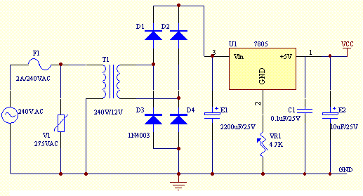
Fuse F1 is used as a protection in case theres any short circuit in the circuit. Varistor V1 is connected in parallel to the input of the line voltage to clamp the surge voltage from the line to a reasonable level that helps to protect the transformer & other circuitry. One time the voltage level surge to a high level beyond the ability of the varistor to absorb it, fuse F1 or varistor V1 or both will burn. If this circuit failed after a period of operation, check that the fuse & the varistor are still in nice condition or else replace them.
Thursday, October 16, 2014
Variable 5 to 20V DC Supply Rise


Sunday, October 5, 2014
TOP245Y 24 W Primary–side Regulated Flyback Power Supply
IC 723 2N3055 13 2V 40A Power Supply Unit

THE HEAVY CURRENT carrying connections are shown in bold in Fig 1. The mains input passes through an EMC filter, protection fuse F1 and ON/OFF switch S 1 to transformer TI. The secondary output of TI is rectified by D I but cannot pass through open relay contacts RL1a. To start the PSU switch, S2 is operated allowing limited current to pass via R1 to slowly charge the reservoir capacitor C1. As C1 charges, the RL1 a pulls in closing the relay contacts and shorting out R1 and S2 placing the PSU in the ON state.
Voltage regulator IC1 is the popular 723. A 7.2V reference on IC 1:6 is fed to non-inverting ICI:5. This is compared with a sample of the PSU output voltage via RI3, RI4 and R15 to inverting input at ICI:4. The 723 can source 150mA at ICl:10, so transistor TR2 acts as a Darlington driver for the pass transistors TR3 to TR7 inclusive. Resistors R21 to R25 are current sharing resistors and the voltage across them is proportional to the current drawn by the PSU load.
When the current through R21 reaches 8A (i.e. a total PSU current output of 40A) the voltage across R11 and R12 is 0.88V and is tapped from R I I to bias a transistor inside IC1 which robs IC1: 10 of some current, forcing the PSU into a current limiting mode.
Saturday, October 4, 2014
Power Supply Adjustable 0 30V

The amount of the ambit is 723 voltage regulator chip circuit. A Darlington brace Q2 Q3 addition the accepted to accord 1A output. The minimum voltage acclimation for this regulator IC is 2 volts aloft V-. Aught volt is accomplished by bartering the V- with a voltage beneath -2V, so the achievement can be adapted to zero. The abrogating accumulation is provided by the apparatus about D3 and D4, counterbalanced by 5.1 Zener diode.
The capricious resistor R3 is acclimated to set the accepted limiter, so your ability accumulation will be save alike back you abbreviate its achievement to ground. To set the aught point, about-face the R11 potentiometer to minimum (counter clockwise) and acclimatize the R12 trimmer potentiometer until the achievement is zero. After this setting, axis the R11 potentiometer to the best will accord about 30V output. If at the best position the achievement is abate than 30V, it’s acceptable acquired by the apparatus tolerance, you can lower the R10 value. Make abiding you use beyond clue for arena affiliation on the PCB, and accommodate acceptable calefaction bore for Q3.
The parts list:
| Item | Quantity | Reference | Part |
|---|---|---|---|
| 1 | 1 | C1 | 470uF/63V |
| 2 | 1 | C2 | 470uF/40V |
| 3 | 1 | C3 | 2200uF/63V |
| 4 | 1 | C4 | 100uF/35V |
| 5 | 1 | C5 | 1nF |
| 6 | 1 | D1 | 5V1 |
| 7 | 1 | D2 | 33V |
| 8 | 4 | D3,D4,D5,D6 | 1N4001 |
| 9 | 1 | D7 | DIODE BRIDGE |
| 10 | 1 | D8 | LED |
| 11 | 1 | F1 | 1.5A |
| 12 | 1 | J1 | PLUG AC MALE |
| 13 | 1 | Q1 | BC557B |
| 14 | 1 | Q2 | BC141 |
| 15 | 1 | Q3 | Q2N3055 |
| 16 | 1 | R1 | 560R |
| 17 | 1 | R2 | 2k2/1W |
| 18 | 2 | R3,R5 | 2k2 |
| 19 | 2 | R10,R6 | 1k2 |
| 20 | 1 | R8 | 100R |
| 21 | 1 | R9 | 0R33/1W |
| 22 | 1 | R11 | POT 10k |
| 23 | 1 | R12 | VR 10k |
| 24 | 1 | R13 | VR 1k |
| 25 | 1 | T1 | 30V 1A |
| 26 | 1 | U1 | LM723 |
Thursday, October 2, 2014
Simple Dual Symmetrical Power Supply Circuit

Tuesday, September 23, 2014
Adjustment power supply values 1 25 15V Max current 0 5 amp circuit
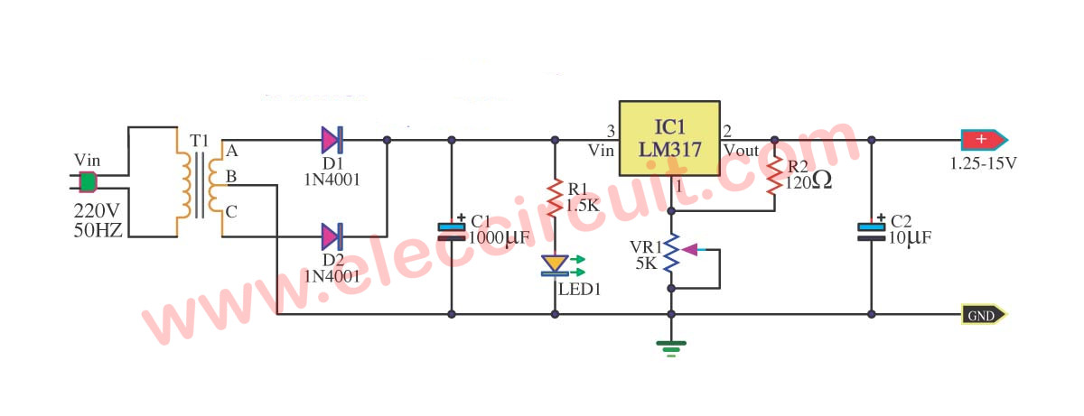
This is power supply that have Voltage output fine the value has 1.25-15V. From by Output current that be valuable about 0.5 amp that 12V and 0.2 amp that 15V.
When Volt , from 220V houses reach transformer. It will modify Volt 220V to be 18VAC already to change rectifier circuit. Which D1, D2, C1 and R1 wasp be Full wave rectifier circuit. For modify DCV to ACV to a signal DCV. It make get a signal DCV that have voltage at pin 3 of IC1 be 20V. From that time DCV signal this reach fight DC Regulator circuit. Which use IC number LM317.
This circuit will perform to maintain one’s position Voltage smoothly. Which level output voltage at get this will go out the way pin 2 of IC1. By have capacitors C2 be voltage filter in order that voltage output level of the circuit is will high class modify to follow fining. The performing fee withstands VR1 there.
from:eleccircuit.com
Sunday, September 21, 2014
30V Variable Power Supply Using LM317
Circuit diagram

Friday, September 19, 2014
Dual Regulated Power Supply
In this schema, the 7815 regulatates the positive supply, and the 7915 regulates the negative supply. The transformer should have a primary rating of 240/220 volts for europe, or 120 volts for North America.
Dual Regulated Power Supply Circuit diagram :

The centre tapped secondary coil should be rated about 18 volts at 1 amp or higher, allowing for losses in the regulator. An application for this type of schema would be for a small regulated bench power supply.
Thursday, September 18, 2014
Simple UPS Power Supply Circuit Diagram
Simple UPS Power Supply Circuit Diagram

Notes:
This circuit can be adapted for other regulated and unregulated voltages by using different regulators and batteries. For a 15 Volt regulated supply use two 12 Volt batteries in series and a 7815 regulator. There is a lot of flexibility in this circuit.
TR1 has a primary matched to the local electrical supply which is 240 Volts in the UK. The secondary winding should be rated at least 12 Volts at 2 amp, but can be higher, for example 15 Volts. FS1 is a slow blow type and protects against short circuits on the output, or indeed a faulty cell in a rechargeable battery. LED 1 will light ONLY when the electricity supply is present, with a power failure the LED will go out and output voltage is maintained by the battery. The circuit below simulates a working circuit with mains power applied:
Between terminals VP1 and VP3 the nominal unregulated supply is available and a 5 Volt regulated supply between VP1 and VP2. Resistor R1 and D1 are the charging path for battery B1. D1 and D3 prevent LED1 being illuminated under power fail conditions. The battery is designed to be trickle charged, charging current defined as :-
(VP5 - 0.6 ) / R1
where VP5 is the unregulated DC power supply voltage.
D2 must be included in the circuit, without D2 the battery would charge from the full supply voltage without current limit, which would cause damage and overheating of some rechargeable batteries. An electrical power outage is simulated below:
Note that in all cases the 5 Volt regulated supply is maintained constantly, whilst the unregulated supply will vary a few volts.
Standby Capacity
The ability to maintain the regulated supply with no electrical supply depends on the load taken from the UPS and also the Ampere hour capacity of the battery. If you were using a 7A/h 12 Volt battery and load from the 5 Volt regulator was 0.5 Amp (and no load from the unregulated supply) then the regulated supply would be maintained for around 14 hours. Greater A/h capacity batteries would provide a longer standby time, and vice versa.
TL494 200W ATX PC Power Supply

Then take a run secondary power supply controlled by transistor Q12 and on his output will be voltage. Behind the voltage regulator IC3 will be voltage 5V, which goes in to the motherboard and it is necessary for turn-on logic and for "Wake on something" functions. Next unstabilized voltage goes through diode D30 to the main control chip IC1 and control transistors Q3 and Q4. When main power supply is running, then this voltage goes from +12V output through diode D.
Thursday, September 11, 2014
Variable DC Power Supply Wiring diagram Schematic
Variable DC Power Supply (Rise) Circuit Diagram
An LED has been put in to the output of the fixed 5V regulator to indicate that the schema is working. Poor soldering is the most likely reason that the schema does not work. Check that all the soldering is done properly. Check that all parts are in their correct position on the PCB. Other items to check are to make sure that the regulators, electrolytic capacitor & bridge rectifier are inserted in the correct orientation.
Parts:
P1____________500R Linear Potentiometer
P2_____________10K Log. Potentiometer

R1,R2___________2K2 1/2W Resistors
R3____________330R 1/4W Resistor
R4____________150R 1/4W Resistor
R5______________1R 5W Resistor

C1___________3300µF 35V Electrolytic Capacitor (see Notes)
C2______________1µF 63V Polyester Capacitor

D1,D2________1N5402 200V 3A Diodes
D3_____________5mm. Red LED

Q1____________BC182 50V 100mA NPN Transistor
Q2____________BD139 80V 1.5A NPN Transistor
Q3____________BC212 50V 100mA PNP Transistor
Q4 __________2N3055 60V 15A NPN Transistor

T1_____________220V Primary, 36V Center-tapped Secondary
 50VA Mains transformer (see Notes)

PL1____________Male Mains plug

SW1____________SPST Mains switch
Wednesday, September 10, 2014
9V Battery Replacement Power Supply
Moreover, the design with the 78L08 and D3 ensures that the voltage regulator is operating in the linear region. The nominal system voltage of 14 V can sometimes sag to about 12 V when heavy loads such as the lights are switched on. Although the schema is obviously suitable for all kinds of applications, we would like to mention that it has been extensively tested on a Yamaha TRX850. These tests show that the converter functions very well and that the interference suppression is excellent. Link