Showing posts with label power. Show all posts
Showing posts with label power. Show all posts
Wednesday, November 5, 2014
4 X 15 Watt Mini Power Amplifier
A lot of electronic circuits in the domain of audio amplifiers are already been published here. This circuit is a little different because it is a four channel amplifier. Each channel of this amplifier can deliver an output of 15Watts into a 4 ohm speaker. The amplifier can be operated from a single 12V DC supply and this makes it possible to use this amplifier in car audio applications too.
4 X 15 Watt Mini Power Amplifier Circuit Diagram :
![4X15W-amplifier-circuit]()
The circuit is based on the 15W BTL X 2 channel audio power amplifier IC TA8215 from Toshiba. Even though chip is specifically designed for car audio applications it can be also used for home audio applications. Two TA8215 ICs are used here in order to obtain a 4 channel amplifier system. The circuit is designed almost exactly as per the application diagram in the ICs datasheet. Pins 7 and 19 are the Vcc pins of the ICs internal integrated power amplifier stages and these pins are connected to the positive supply. Pin 9 is the Vcc pin for ICs internal preamplifier and it is also connected to the positive supply. Pins 13 and 14 are the internal power amplifiers ground pins and they are tied together and connected to the ground.
The internal preamplifier’s ground pin (pin5) is connected to the common ground through a 10 Ohm resistor which makes the input ground separated from the common ground by a resistance of 10 ohms and this improves the noise rejection. The 100uF capacitor works as a power supply de-coupler. The resistor networks connected to the output lines of each amplifier improves the high frequency stability. The variable resistors (R3, R4, R12 and R13) works as the volume controller for the corresponding channels.
Notes :
4 X 15 Watt Mini Power Amplifier Circuit Diagram :
The internal preamplifier’s ground pin (pin5) is connected to the common ground through a 10 Ohm resistor which makes the input ground separated from the common ground by a resistance of 10 ohms and this improves the noise rejection. The 100uF capacitor works as a power supply de-coupler. The resistor networks connected to the output lines of each amplifier improves the high frequency stability. The variable resistors (R3, R4, R12 and R13) works as the volume controller for the corresponding channels.
Notes :
- Assembling the circuit on a good quality PCB is a must for obtaining optimum sound quality.
- Use 12V DC for powering the circuit.
- The ICs must be fitted with adequately sized heat sinks.
- R3, R4, R12 and R13 serves as volume controllers.
- K1 to K4 can be 4 Ohm, 20W speakers.
- This amplifier circuit can be used in a variety of applications such as car audio systems, home theater systems, personal audio systems, public address systems etc.
Tuesday, November 4, 2014
Stereo Power Amplifier Circuit based on BA5417
BA5417 is a stereo amplifier IC with a lot of good features like thermal shut down, standby function, soft clipping, wide operating voltage range etc. The IC can deliver 5W per channel into 4 ohm loud speakers at 12V DC supply voltage. The BA5417 has excellent sound quality and low THD (total harmonic distortion) around 0.1% at F=1kHz; Pout=0.5W.
Stereo Power Amplifier Circuit diagram :
Setup and working of this stereo power amplifier circuit is somewhat similar to the BA5406 based stereo amplifier circuit published previously. C10 and C11 are DC decoupling capacitors which block any DC level present in the input signals. C2 and C6 couples the amplifiers left and right power outputs to the corresponding loud speakers. C1 and C5 are bootstrap capacitors.
Bootstrapping is a method in which a portion of the amplifiers is taken and applied to the input. The prime objective of bootstrapping is to improve the input impedance. Networks R1,C3 and R2,C7 are meant for improving the high frequency stability of the circuit. C4 is the power supply filter capacitor. S1 is the standby switch. C8 is a filter capacitor. R3 and R4 sets the gain of the left and right channels of the amplifier in conjunction with the 39K internal feedback resistors.
Note :
- Supply voltage range of BA5417 is from 6 to 15V DC.
- The recommended supply voltage for this circuit is 12V DC.
- The power supply must be well regulated and filtered.
- BA5417 requires a heatsink.
- The circuit can be assembled on a perf board without much degradation in performance.
Sunday, November 2, 2014
IRF740 Datasheet power MOSFET
N - CHANNEL 400V - 0.48 Ω - 10 A - TO-220
PowerMESH MOSFET
This power MOSFET is designed using the company’s consolidated strip layout-based MESH OVERLAY process. This technology matches and improves the performances compared with standard parts from various sources.
APPLICATIONS
# HIGH CURRENT SWITCHING
# UNINTERRUPTIBLE POWER SUPPLY (UPS
# DC/DC COVERTERS FOR TELECOM,
# INDUSTRIAL, AND LIGHTING EQUIPMENT

MOSFET, N, 400V, 10A, TO-220; Transistor Type:MOSFET; Transistor Polarity:N; Voltage, Vds Typ:400V; Current, Id Cont:10A; Resistance, Rds On:0.55ohm; Voltage, Vgs Rds on Measurement:10V; Voltage, Vgs th Typ:4V; Case Style:TO-220AB; Termination Type:Through Hole; Current, Idm Pulse:40A; Power Dissipation:125W; Power, Pd:125W; Thermal Resistance, Junction to Case A:1 C/W; Voltage, Vds Max:400V
Read More..
PowerMESH MOSFET
This power MOSFET is designed using the company’s consolidated strip layout-based MESH OVERLAY process. This technology matches and improves the performances compared with standard parts from various sources.
APPLICATIONS
# HIGH CURRENT SWITCHING
# UNINTERRUPTIBLE POWER SUPPLY (UPS
# DC/DC COVERTERS FOR TELECOM,
# INDUSTRIAL, AND LIGHTING EQUIPMENT
MOSFET, N, 400V, 10A, TO-220; Transistor Type:MOSFET; Transistor Polarity:N; Voltage, Vds Typ:400V; Current, Id Cont:10A; Resistance, Rds On:0.55ohm; Voltage, Vgs Rds on Measurement:10V; Voltage, Vgs th Typ:4V; Case Style:TO-220AB; Termination Type:Through Hole; Current, Idm Pulse:40A; Power Dissipation:125W; Power, Pd:125W; Thermal Resistance, Junction to Case A:1 C/W; Voltage, Vds Max:400V
Saturday, November 1, 2014
9V Battery Replacement Power Supply Circuit Diagram
This circuit was originally designed to power a motorcycle intercom from the vehicle supply system. This type of intercom, which is used for communication between driver and passenger, generally requires quite a bit of power. In order to improve intelligibility there is often elaborate filtering and a compander is sometimes used as well. The disadvantage is that a battery doesn’t last very long. You could use rechargeable batteries, of course, but that is often rather laborious. It seems much more obvious to use the motorcycle power supply instead. A 9-V converter for such an application has to meet a few special requirements.
9V Battery Replacement Power Supply Circuit Diagram
![9V]()
9V Battery Replacement Power Supply Circuit Diagram
For one, it has to prevent interference from, for example, the ignition system reaching the attached circuit. It is also preferable that the entire circuit fits in the 9-V battery compartment. This circuit meets these requirements quite successfully and the design has nonetheless remained fairly simple. In the schematic we can recognize a filter, followed by a voltage regulator and a voltage indicator. D1, which protects the circuit against reverse polarity, is followed by an LC and an RC filter (C3/L1/L2/C1/R1/C2). This filter excludes various disturbances from the motorcycle power system.
Moreover, the design with the 78L08 and D3 ensures that the voltage regulator is operating in the linear region. The nominal system voltage of 14 V can sometimes sag to about 12 V when heavy loads such as the lights are switched on. Although the circuit is obviously suitable for all kinds of applications, we would like to mention that it has been extensively tested on a Yamaha TRX850. These tests show that the converter functions very well and that the interference suppression is excellent.
Thursday, October 30, 2014
20A Transformerless Power Supply
| 20A Transformerless Power Supply |
This PSU has been abnormally advised in place of current-hungry ham telephone system transceivers. It delivers vigilantly in relation to 20Amps on 13.8V. For cut currents, a distant received attached output, able of 15ma up to a absolute of 20A has been added. accede to us ensure what did you say? we consent got at this time. The skill agent must remain able to bear by atomic 25A at 17.5 to 20V. The reduce the voltage, the lower power dissipation. The rectified conventional willpower be �ironed� by the C1, whose accommodation ought to not be beneath than 40.000uF, (a aureate adage of nearly 2000uF/A), but we give enthusiastic approval to up to 50.000uF. This accommodation can subsist present at birth up by several abate capacitors inside congruence. The wretched of this architecture is a trouble-free 12V supervisor (7812). The achievement voltage can be brought to adapted amount (now 13.8V) by two alien resistors (R5 and R6) claim this formula:
U= 12(1+R5/R6)
The low currents (at this time 15mA) self-control accumulate the 7812 in its permitted function. for instance shortly as the customary rises greater than 15ma, the voltage bead on R4 will amenable the Q3, certainly administration the aerial achievement current. This is a PNP transistor (Ic>25) and established addition agency of next to atomic 20. The lone with the intention of has been activated and accurate reality is the 2N5683. The acknowledged attached attrition RL, in support of the superlative achievement of 20 Amps be supposed to take place 0.03 Ohms, rated by
slightest 15W. You can help the attrition wire or else in relation to-cope with several resistors clothed in comparable, increase the resistance/power ideals. Ethics used for added currents can be affected by the government:
RL=0.7/Imax
The RL and Q2 (3A PNP such in the same way as BD330) anatomy a abbreviate ambit automatic fuse. As in a bit as the preeminent usual alcove 20Amps, the voltage bead in excess of the resistor RL wish simple Q2, and appropriately absolute the B-E time-honored of Q3. Alongside to Q2 is Q1, which light the LED 1 when the accepted attached ambit is dynamic. what time the �fuse� is active, the Q2 bridges the R3, so the wealthy normal would breeze through the IC1, and accident it. Therefore the R4 is inserted, being to absolute the IC1 accepted to 15mA. This makes it understandable to run the IC1 afterwards one cooling aid. The LED 2 force alight up all spell the PSU is switched on.
in attendance is an modifiable normal limiter popular alongside to the anchored output, appropriately accouterment regulating accepted precursor on behalf of abate currents.
This ambit is authentic down-to-earth too. You desire apprehension to in attendance is refusal acknowledged analysis resistor. But it is totally here, in a anatomy of the Rds-on attrition of the N-channel FET, which absolutely handles the amount blow from the source. The exploit of the FET is perceptible featuring in the diagram 2. as the established Id is rising, the astriction Uds on top of the attrition Rds rises definite boring in the commencement, but actual fast afterwards the knick. This agency, to afore the knick the FET behaves what a resistor but afterwards it, facility as connected acknowledged source.
The D2, R3 and B-E connection of the Q4 desire faculty the Uds voltage of the FET1. what time the voltage rises sufficient, the Q4 will adjustment the FET1 aboideau to majority, and scratch the expected breeze through the FET 1 rotten. However, to sanction the FET1 to sincere, in attendance is assertive aboideau voltage crucial, which during this occurrence is brought up by the voltage link consisting of R8, Z1, P1 and R9. So the finest Aboideau voltage desire ensue the single of the Z1, and the basal will be something like 3V6. The Z1 voltage (Uz1) will appropriately actuate the do well standard affluent through the FET 1.
The diagram 2 will outer shell to facilitate pro 5 Amps the Uz1 ought to come to pass 5V6, and for 20Amps about 9V6. The Capacitor C4 desire actuate the velocity otherwise the acknowledgment point of the limiter. 100 uF will accomplish the acknowledgment time to be nearly 100ms, and 1n will accomplish it 1us.
inside the advised limits, the P1 resolve absolute the customary achievement at home the ambit of 15mA to 20A. You can handle both achievement concurrently, but the absolute achievement time-honored will come to pass bound by the amount of the RL. This PSU can be habitual additionally in lieu of college outputs, while continued as the agent yearn for lever the standard food, and you accommodate acceptable cooling for the Q3.
source : www.electronics-lab.com
Monday, October 27, 2014
Most Power Supply for Amplifier
As with most power amplifiers, the ±60 V power supply need not be regulated. Owing to the relatively high power output, the supply needs a fairly large mains transformer and corresponding smoothing capacitors—see circuit diagram below.
Read More..
 |
| Note that the supply shown is for a mono amplifier; a stereo outfit needs two supplies. |
The power supply is straightforward, but can handle a large current. Voltage acserves as drive for the power-on delay circuit. The transformer is a 625 VA type, and the smoothing capacitors are 10 000 µF, 100 V electrolytic types. The bridge rectifier needs to be mounted on a suitable heat sink or be mounted directly on the bottom cover of the metal enclosure.. The transformer needs two secondary windings, providing 42.5 V each. The prototype used a toroidal transformer with 2x40 V secondaries. The secondary winding of this type of transformer is easily extended: in the prototype 4 turns were added and this gave secondaries of 2x42.5 V.
60W Dual Stereo Power Amplifier
A portion of electronic circuits into the domain of audio amplifiers are already been available at this juncture. This circuit is a hardly singular for the reason that it is a four channel amplifier. each one channel of this amplifier can furnish with an output of 15Watts into a 4 ohm amplifier. The amplifier can subsist operated from a single 12V DC supply and this makes it likely to spend this amplifier happening car audio applications too.
The circuit is based on the 15W BTL X 2 channel audio power amplifier IC TA8215 from Toshiba. Even though whittle is specifically designed designed for car audio applications it can stay and used for to your place audio applications. Two TA8215 ICs are used now in order to gain a 4 channel amplifier practice. The circuit is designed almost exactly in the role of for each the use diagram within the ICs datasheet. Pins 7 and 19 are the Vcc pins of the ICs inner integrated power amplifier stages and these pins are connected to the optimistic supply. Pin 9 is the Vcc pin in lieu of ICs interior preamplifier and it is additionally connected to the positive supply.
 |
| 60W Dual Stereo Power Amplifier |
Pins 13 and 14 are the domestic power amplifiers ground pins and they are fixed cool and connected to the ground. The in-house preamplifier’s ground pin (pin5) is connected to the regular ground through a 10 Ohm resistor which makes the input ground separated from the common ground by a resistance of 10 ohms and this improves the sound rejection. The 100uF capacitor workings in the function of a power supply de-coupler. The resistor networks connected to the output defenses of both amplifier improves the far above the ground frequency stability. The movable resistors (R3, R4, R12 and R13) facility as the volume controller intended for the corresponding channels.
Saturday, October 25, 2014
Power Monitor Non Contact Diagram Circuit
Here is a simple non-contact AC power monitor for home appliances and laboratory equipment that should remain continuously switched-on. A fuse failure or power breakdown in the equipment going unnoticed may cause irreparable loss. The monitor sounds an alarm on detecting power failure to the equipment. The circuit is built around CMOS IC CD4011 utilising only a few components. NAND gates N1 and N2 of the IC are wired as an oscillator that drives a piezobuzzer directly. Resistors R2 and R3 and capacitor C2 are the oscillator components. The amplifier comprising transistors T1 and T2 disables the oscillator when mains power is available. In the standby mode, the base of T1 picks up 50Hz mains hum during the positive half cycles of AC and T1 conducts.
 This provides base current to T2 and it also conducts, pulling the collector to ground potential. As the collectors of T1 and T2 are connected to pin 2 of NAND gate N1 of the oscillator, the oscillator gets disabled when the transistors conduct. Capacitor C1 prevents rise of the collector voltage of T2 again during the negative half cycles. When the power fails, the electrical field around the equipment’s wiring ceases and T1 and T2 turn off. Capacitor C1 starts charging via R1 and preset VR and when it gets sufficiently charged, the oscillator is enabled and the piezobuzzer produces a shrill tone. Resistor R1 protects T2 from short circuit if VR is adjusted to zero resistance.
The circuit can be easily assembled on a perforated/breadboard. Use a small plastic case to enclose the circuit and a telescopic antenna as aerial. A 9V battery can be used to power the circuit. Since the circuit draws only a few microamperes current in the standby mode, the battery will last several months. After assembling the circuit, take the aerial near the mains cable and adjust VR until the alarm stops to indicate the standby mode. The circuit can be placed on the equipment to be monitored close to the mains cable
This provides base current to T2 and it also conducts, pulling the collector to ground potential. As the collectors of T1 and T2 are connected to pin 2 of NAND gate N1 of the oscillator, the oscillator gets disabled when the transistors conduct. Capacitor C1 prevents rise of the collector voltage of T2 again during the negative half cycles. When the power fails, the electrical field around the equipment’s wiring ceases and T1 and T2 turn off. Capacitor C1 starts charging via R1 and preset VR and when it gets sufficiently charged, the oscillator is enabled and the piezobuzzer produces a shrill tone. Resistor R1 protects T2 from short circuit if VR is adjusted to zero resistance.The circuit can be easily assembled on a perforated/breadboard. Use a small plastic case to enclose the circuit and a telescopic antenna as aerial. A 9V battery can be used to power the circuit. Since the circuit draws only a few microamperes current in the standby mode, the battery will last several months. After assembling the circuit, take the aerial near the mains cable and adjust VR until the alarm stops to indicate the standby mode. The circuit can be placed on the equipment to be monitored close to the mains cable
3000 watt power inverter 12V DC to 230V AC
3000 watt power inverter 12V DC to 230V AC
 |
| Circuit Diagram of 3000 watt power inverter 12V DC to 230V AC |
 |
| Fig. 2: Sine-wave voltage and conventional square wave voltage with both 230 Volt rms |
 |
| Fig. 3: Square wave voltage with duty cycle 25% for 230 Volt rms ("modified sine") |
PCB Layout:3000 watt power inverter 12V DC to 230V AC

Component Placement: 3000 watt power inverter 12V DC to 230V AC

 |
| fig.: output voltage with no load or inductive load. |
 |
| fig.: resistor 0,001 Ohm made of high-grade steel sheet metal |
Control electronics | 3000 watt power inverter 12V DC to 230V AC

 |
| fig.: control electronics on strip hole plate (previous version) and PCB of the "professional edition" |
Assembly of the mosfet-transistors on the heat sink | 3000 watt power inverter 12V DC to 230V AC

 |
| fig.: heat sink, mosfet transistors, connections. |
Final assembly | 3000 watt power inverter 12V DC to 230V AC

 |
| fig.: 1500 VA inverter with 2 parallel transformers and 1000 VA inverter |
Source:http://www.qsl.net
Friday, October 24, 2014
12 Volt DC Power Suplly Adaptor
This series of images you can apply to make an adapter or power suplly with the output voltage (V DC output 12V). Power supply in the only protected by a capacitor as a safety if the power supply is connected to the load on the circuit.

So I recommend using 35V capacitor with a minimum specification. The security of power supply to power the more we can menggunakkan transistor TIP, but I have not discussed it. To the diode bridge can be compiled from the 4 then you solder the diode bridge rectifier into one or you can buy a bridge rectifier so that the comb-shaped (sideways) or the box. At least I would suggest using a diode bridge 1 Ampere, in a series of adapters, the bigger the better course of ampere diode current in the circuit. Diodes like toll roads, and current as a car passing by. The larger and the width of the existing highway, the faster the flow of runs and through the circuit.
For the circuit power supply 5 V, you can change the volt regulator on the type 7805 and 7905. This application applies equally in this series. For variations such as fuse or circuit switch on / off you can try it yourself.
Transformer 18 V + - 1 A minimum CT
Minimum of 35 V + Capacitor
Adjustable Symmetrical Power Supply Using LM317 and LM337
The circuit was designed to provide an adjustment with a power supply that is symmetrically designed while providing a voltage range of 1.25V to 30V at 1A current. LM317 – an adjustable 3-terminal positive voltage regulator capable of supplying in excess of 1.5A over an output voltage range of 1.2V to 37V and requires only two external resistors to set the output voltage due to its internal current limiting, thermal shutdown and safe area compensation, making it essentially blow-out proof LM337 – an adjustable 3-terminal positive voltage regulator capable of supplying in excess of 5A used as battery chargers, constant current regulators, and adjustable power supplies due to its features such as protected output from short circuit, product enhancement tested, current limit constant with temperature, guaranteed thermal regulation, adjustable output down to 1.2V, guaranteed 5A, and guaranteed 7A peak output current.

The circuit will serve as a voltage converter with an input voltage of 35 V to produce an output voltage of 1.25 V to 30 V. The positive voltage is being handled by LM317 IC while the negative voltage is handled by LM337. The circuit can provide an output current of 1 A. During the production of 1 A current, the regulator is dissipating too much heat and without the presence of a heatsink, the regulator may get damaged.
Using these types of regulators provide features such as low noise and low price in the market. It can be made operational even with few components used. The only disadvantage that it will impose is the poor conversion efficiency. With the output of 35 V to 5 V, the efficient ratio of the output power with the input power is less than 42%. This is the reason why the switching regulator became cheap recently although the number of external components to be connected is minimally increased. These regulators will work with better efficiency when used in case where current is more than 1A for more than 15 V and 0.4 A for less than 15 V from the power supply. Each regulator is adjusted for single positive and negative voltage output using the 10K ohms potentiometers RV1 & RV2. For dual outputs, a dual connected potentiometer RV3 is made to operate by switch S1. The visual indication on the voltmeter V1 is shown using the switch S2.
Using these types of regulators provide features such as low noise and low price in the market. It can be made operational even with few components used. The only disadvantage that it will impose is the poor conversion efficiency. With the output of 35 V to 5 V, the efficient ratio of the output power with the input power is less than 42%. This is the reason why the switching regulator became cheap recently although the number of external components to be connected is minimally increased. These regulators will work with better efficiency when used in case where current is more than 1A for more than 15 V and 0.4 A for less than 15 V from the power supply. Each regulator is adjusted for single positive and negative voltage output using the 10K ohms potentiometers RV1 & RV2. For dual outputs, a dual connected potentiometer RV3 is made to operate by switch S1. The visual indication on the voltmeter V1 is shown using the switch S2.
- R1-2=270ohms
- R3-4=2.2Kohms
- R5-6=10Kohms
- C1-5=100uF/63V
- C2-4=100nF/100V
- C3-8=10uF/25V
- C6-10=100uF/63V
- C7-9=100nF/100V
- RV1-2=10Kohms Lin.
- RV3=2X10Kohms Lin.
- IC 1=LM 317T
- IC 2=LM 337T
- D1-2=1N4001
- D3-4=1N4001
- L1-2=LED 3mm
- F1-2=1A slow Blow Fuse
- S1-2=2X ON-ON SW
- V1=0-30V DC Voltmeter
The adjustable symmetrical power supply is suitable to be used in audio amplifiers, microphone amplifiers, op-amp applications, impedance converters and other devices that require regulated positive and negative DC supply, since the output current is 1 A.
Thursday, October 23, 2014
12Volt Transformerless power supply
This is a 12V 100mA Transformerless power supply in support of low current applications. C1 is the X rated AC capacitor so as to reduces climax volt AC. D1-D4 rectifies AC to DC and C2 removes ripples. R1 is the bleeder to remove stored current clothed in AC while power is rancid. R2 limits inrush current. A Zener can stay used in the output to pick up regulated DC.
| 12V 100mA Transformerless power supply Circuit Diagram |
Electricity Power Saver
Do you know how to work his usual power saving devices in the market is shaped like a dry battery with a plug into an outlet?. Actually you can create your own tool with much better quality with much cheaper price.
Because of the way it works is to reduce the magnitude from cosine curve AC current that will be read on the gauge kilometer. Device work if there is air conditioning load passes through a coil of wire sensors to measure the AC current which is being passed.
Because of the way it works is to reduce the magnitude from cosine curve AC current that will be read on the gauge kilometer. Device work if there is air conditioning load passes through a coil of wire sensors to measure the AC current which is being passed.
 |
| Power Saver Circuit |
1 3V DC to 12 2V DC Regulator Power Supply
Power supply circuit to generate output below were variations between 1.3V DC to 12.2V DC with 1A current.
In addition, the power supply circuit is also equipped with over-current protection or shield against belebih flow. Power supply circuit is very simple, but the quality is quite good, made her basiskan regulator IC LM723 is a pretty legendary.
In addition, the power supply circuit is also equipped with over-current protection or shield against belebih flow. Power supply circuit is very simple, but the quality is quite good, made her basiskan regulator IC LM723 is a pretty legendary.

Description:
R2 to set the output voltage. The maximum current is determined by R3, over-current protection circuit inside the LM723 to detect the voltage on R3, if it reaches 0.65 V, the voltage output will be off her. So the current through R3 can not exceed 0.65 / R3 although output short-circuit in his.
C3 and C4 are ceramic capacitors, as much as possible directly soldered to the PCB, this is because the LM723 is prone to oscillation that is not cool.
LM723 works with 9.5V input voltage to 40 V DC and the LM723 can generate its own current of 150mA when the output voltage is not more than 6-7V under input voltage.
Specifications:
Output (value estimated):
Vmin = (R4 + R5) / (R5 * 1.3)
Vmax = (7.15 / R5) * (R4 + R5)
Imax = 0.65/R3
Max. Power on R3: 0.42/R3
Min. DC Input Voltage (pin 12 to pin 7): Vmax + 5
Component List:
B1 40V/2.5A
C1 2200uF (3300uF even better)
C2 4.7uF
C3 100nF
C4 1NF
C5 330nF
C6 100uF
Green LED D1
D2 1N4003
F1 0.2A F
F2 2A M
IC1 LM723 (in a DIL14 plastic package)
R1 1k
R2 Pot. 5k
R3 0.56R/2W
R4 3.3k
R5 4.7k
S1 250V/1A
T1 2N3055 on a heatsink 5K / W
TR1 220V/17V/1.5
Monday, October 20, 2014
Simple 8 Watt Audio Power Amplifier Schematic
Here is the schematic for an 8 watt audio power amplifier. This amp can be used as a simple booster, the heart of a more complicated amplifier or used as a guitar amp. It is very small and portable unit and can be powered through 12V battery. I built the circuit on a Vero Board and had to add extra inductors, capacitors and resistors to prevent oscillation.
Circuit diagram:

8 Watt Audio Power Amplifier Circuit Diagram
Parts:
R1 = 47K
R2 = 2.2R/1W
R3 = 220R/1W
R4 = 2.2R/1W
C1 = 100nF-63V
C2 = 10uF-25V
C3 = 470uF-25V
C4 = 2000uF-25V
C5 = 100nF-63V
IC1 = LM383
SPKR = 4ohm/8W
Notes:
- IC1 must be installed on a heat sink.
- C1 is for filtering and to prevent oscillation and should not be omitted.
- The circuit can be built on a Vero Board, universal solder board or PC board, the PC board is preferred.
- The circuit draws about 880Ma at 12 V.
- By swapping the values of R2 and R3; you can turn this amplifier into a guitar amp with no preamp required.
- If you cant find 2000uF, then replace C4 with a 2200uF unit.
- If you add a 0.2uF capacitor in series with a 1 ohm resistor to the output you can prevent oscillation of the circuit under certain conditions.
Automatic Low Power Emergancy Light Circuit diagram
Here is a white-LED-based emergency light that offers the following advantages. 1-It is highly bright due to the use of white LEDs. 2-The light turns on automatically when mains supply fails, and turns off when mains power resumes. 3-It has its own battery charger. When the battery is fully charged, charging stops automatically. The charger power supply section is built around 3-terminal adjustable regulator IC LM317 (IC1), while the LED driver section is built around transistor BD140 (Q2).
In the charger power supply section, an input AC main is stepped down by T1 to deliver 9V, 500mA to the bridge rectifier, which comprises diodes D1 through D4. Filter capacitor C1 eliminates ripples. Unregulated DC voltage is fed to input pin 3 of IC1 and provides charging current through D5 and limiting resistor R15. By adjusting preset P1, the output voltage can be adjusted to deliver the required charging current. When the battery gets charged to 6.8V, D6 conducts and charging current from IC1 finds a path throughQT1 to ground and it stops charging of the battery. When mains power is available, the base of Q2 remains high and Q2 does not conduct. Thus LEDs are off.
On the other hand, when mains fails, the base of Q2 becomes low and it conducts. This makes all the LEDs glow. The mains power supply, when available, charges the battery and keeps the LEDs off as Q2 remains cut-off. During mains failure, the charging section stops working and the B1 supply makes the LEDs glow. Assemble the circuit on a general-purpose PCB and enclose in a cabinet with enough space for battery and switches. We have tested the circuit with twelve 10mm white LEDs. You can use more LEDs provided the total current consumption does not exceed 1.5A. Driver transistor Q2 can deliver up to 1.5A with proper heat-sink arrangement.
Circuit diagram:

Fully Automatic Emergency Light Circuit Diagram
Parts:
P1 = 2.2K
R1-R12 = 100R-1/2W
R13 = 1K-1/2W
R14 = 180R-1/2W
R15 = 16R/5W
R16 = 1.2K
C1 = 1000uF-25V
D1-D5 = 1N4007
D6 = 6.8V-0.5W Zener
D7-D18 = 10mm- White LEDs
Q1 = BC548
Q2 = BD140
B1 = 6V-4.5Ah Battery
IC1 = LM317
T1 = 9Vac-Transformer
P1 = 2.2K
R1-R12 = 100R-1/2W
R13 = 1K-1/2W
R14 = 180R-1/2W
R15 = 16R/5W
R16 = 1.2K
C1 = 1000uF-25V
D1-D5 = 1N4007
D6 = 6.8V-0.5W Zener
D7-D18 = 10mm- White LEDs
Q1 = BC548
Q2 = BD140
B1 = 6V-4.5Ah Battery
IC1 = LM317
T1 = 9Vac-Transformer
Friday, October 17, 2014
Stabilized Regulated Power Supply Circuit Diagram
This circuit of power supply, is very simple and easy to built, it can be assembled on a general-purpose PCB, finding its materials is very easy and cost-small. The output voltage is stabilized and is regulated in the region from 0V until + 15V dc, with biggest provided current 1 A. The regulation becomes with the P1. The Q1 is classic power transistor and it needs to be placed on a cool rib (Heatsink), when it works continuously in the region of biggest current it gets hot. The type of transformer is standard in the market.
Circuit diagram:

Stabilized Power Supply Circuit Diagram
Parts:
P1 = 330R-Potentiometer
R1 = 560R-2W
C1 = 2200uF-35V
C2 = 100uF-35V
C3 = 10uF-25V
C4 = 220uF-25V
C5 = 100nF-63V
D1 = 18V-1.5W Zener
Q1 = 2N3055 NPN Transistor
T1 = 220VAC – 18V@ 1.5A
BR1 = 4x1N4007 Diode Bridge
SW1 = Mains On-Off Switch
5 to 15V Regulated Power Supply
Regulated Power Supply
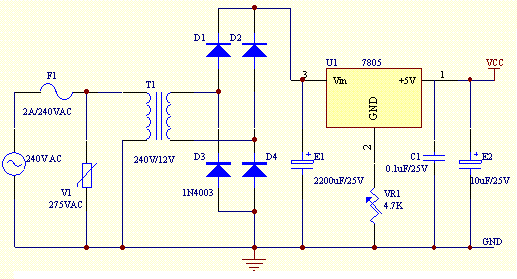
Fuse F1 is used as a protection in case theres any short circuit in the circuit. Varistor V1 is connected in parallel to the input of the line voltage to clamp the surge voltage from the line to a reasonable level that helps to protect the transformer & other circuitry. One time the voltage level surge to a high level beyond the ability of the varistor to absorb it, fuse F1 or varistor V1 or both will burn. If this circuit failed after a period of operation, check that the fuse & the varistor are still in nice condition or else replace them.
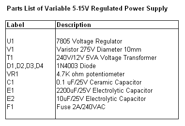
This project is a normal DC regulated power supply that is a variable DC voltage range from 5V to 15V. It can supply current up to 400mA to power the various circuits for your electronic projects. The voltage output is varied by using the potentiometer V.R1. In this circuit, the input line power supply is designed for 240V.A.C. If 110VAC input is used, alter the ratings of the varistor to 150VAC & the transformer ratio to 110V/12V.
Fuse F1 is used as a protection in case theres any short circuit in the circuit. Varistor V1 is connected in parallel to the input of the line voltage to clamp the surge voltage from the line to a reasonable level that helps to protect the transformer & other circuitry. One time the voltage level surge to a high level beyond the ability of the varistor to absorb it, fuse F1 or varistor V1 or both will burn. If this circuit failed after a period of operation, check that the fuse & the varistor are still in nice condition or else replace them.
Diodes D1, D2, D3 and D4 are used to rectify the 12V.A.C voltage to DC voltage. Electrolytic capacitor E1 is used as a smoothing capacitor to reduce the ripple of the DC voltage. The DC voltage is fed in to the input of 7805 regulator where the output DC voltage is obtained. Changing the worth of VR1 will alter the output of the DC voltage. Capacitor C1 is used to filter out high frequency part from the power supply.
Thursday, October 16, 2014
Simple Complementary Push Pull Power Amplifier Circuit
This amplifier circuit is very popular audio power amplifier circuit type. We call it a complementary since the final transistors is an NPN-PNP pair, each with the same characteristics. This circuit produce an AB class amplifier, since each transistor works in slightly more than half cycle of the signal. There is overlap area when both transistor conduct a current, and this area will be around its stationary current (when the input signal is zero). This circuit is also known as push-pull amplifier circuit since each transistor in the pair is working alternatively. Here is the schematic diagram of the circuit:
Complementary (Push-Pull) Power Amplifier Circuit Diagram
+Power+Amplifier+Circuit.gif "Complementary")
Wednesday, October 15, 2014
Audio Power Amplifier for AM Radio Circuit Diagram
This is an AM radio power amplifier circuit. What is different with other general amplifier is that this circuit has a low-pass filter (passive type), built using R1C1 to limit the input-output frequency response. Additionally, a ferroxcube K5-001-001/3B with 3 turns of wire is used as ferrite bead at output filter. All components should be spaced very close to the IC.
The ground and speaker lead must be twisted tightly. The supply lead and supply ground also must be twisted very tightly. Here is the schematic diagram of the circuit.
Audio Power Amplifier for AM Radio Circuit Diagram

Subscribe to:
Posts (Atom)