Showing posts with label digital. Show all posts
Showing posts with label digital. Show all posts
Saturday, October 25, 2014
Digital Volume Control Circuit Diagram
This circuit could be used for replacing your manual volume control in a stereo amplifier. In this circuit, push-to-on switch SW1 controls the forward (volume increase) operation of both channels while a similar switch SW2 controls reverse (volume decrease) operation of both channels. A readily available IC from Dallas semiconductor, DS1669 is used here.
Circuit Diagram:

Parts:
J1 = RCA Audio Input Socket
J2 = RCA Audio Input Socket
C1 = 0.1uF-16V Ceramic Disc Capacitor
C2 = 0.1uF-16V Ceramic Disc Capacitor
C3 = 0.1uF-16V Ceramic Disc Capacitor
IC1 = DS1669 (is available from Dallas SCo.
SW1 = Momentary Push Button Switch
SW1 = Momentary Push Button Switch
Notes:
Circuit Diagram:

Digital Volume Control Circuit Diagram
Parts:
J1 = RCA Audio Input Socket
J2 = RCA Audio Input Socket
C1 = 0.1uF-16V Ceramic Disc Capacitor
C2 = 0.1uF-16V Ceramic Disc Capacitor
C3 = 0.1uF-16V Ceramic Disc Capacitor
IC1 = DS1669 (is available from Dallas SCo.
SW1 = Momentary Push Button Switch
SW1 = Momentary Push Button Switch
Notes:
- Replaces mechanical variable resistors.
- Electronic interface provided for digital as well as manual control.
- Wide differential input voltage range between 4.5 and 8 volts.
- Wiper position is maintained in the absence of power.
- Low-cost alternative to mechanical controls.
- Applications include volume, tone, contrast, brightness, and dimmer control.
- The circuit is extremely simple and compact requiring very few external components.
- The power supply can vary from 4.5V to 8V.
- The input signal should not fall below -0.2 volts.
Friday, October 24, 2014
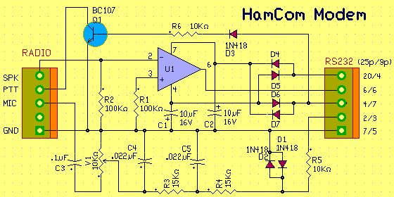
Modem for Digital Modes Circuits Diagram
Ham Com is a modem for almost all types of digital transmission for radio amateurs. It can be used to RTTY, ASCII, NevTex, Sitor, Amtor, Fec, CW, FSK, etc.. The modem is simple and can even be used for receiving faxes and SSTV wx-using JV-FAX software.
Modem for Digital Modes Circuits Diagram

To use this modem, you need a PC with serial port, Software HamCom and radio equipment.
Modem for Digital Modes Circuits Diagram

To use this modem, you need a PC with serial port, Software HamCom and radio equipment.
Friday, October 17, 2014
What is CMOS Digital Electronics Technology C MOS
C-MOS or CMOS stands for complementary metal-oxide-semiconductor, it is a technology for constructing integrated circuits widely used in microprocessors, microcontrollers, and other Digital Memory RAM circuits. CMOS technology is also used for several analog circuits such as image sensors, data converters and transceivers for many types of communication. Created by Frank Wanlassem 1963, CMOS is also sometimes referred to as complementary-symmetry metal-oxide-c or COS-MOS semiconductor. The words "complementary-symmetry" refer to the fact that the typical digital design style with CMOS uses complementary and symmetrical pairs of field effect transistors (Field Effect Transistors - FET) p-type or n semiconductor oxide metal (MOSFETs) for logic functions, as shown in figure below.
What is CMOS
Existem features relevant and important in CMOS devices such as low immunity to static and low energy consumption. As one of the transistor pair is always turned off, the combinação em series consumes significant energy only momentarily during the alternation between connected and disconnected states (on / off). Consequentemente, CMOS devices NON produzem much heat as other forms of rationale, such as TTL, which typically consume current even quando em home.
The também CMOS technology enables high-density u funções em um logic single chip. It was mainly for this race that has become the most used technology to be applied em VLSI (Very-large-scale Integration), is the Process of criação integrated circuit through the combinação of milhares transistor em um single chip.
Family CMOS integrated circuits - 4000 and 74C
The 4000 series is a family of CMOS integrated circuits that implement a variety of logic functions that are still in use today . They were introduced by RCA as CD4000 series COS / MOS in the year 1968 as a lower power and a more versatile alternative to the 7400 series TTL . This CMOS series have the advantage of lower power consumption and wide range of supply voltages of 3 V to 15 V . However its speed is slower , 1 MHz , compared to the 10 MHz bipolar TTL , this limits their applications to projects of low speed or static .
Characteristics CMOS
Supply ( Vdd ) : as the supply voltage , this family allows for series 4000 and 74C operating in the range of 3V to 15V , for the HC version of 2V to 6V and HCT of 4.5 V to 5.5 V. For series low voltage , the range is from 1V to 3.6V and 1.2V to LV to 3.3 V , typical voltage of various current systems .
Integrated circuits CMOS Whenever there unused entries or entire unused ports , it is critical that all inputs are grounded or connected to + VDC , we have to take this step due to
large impedance inputs 10 ¹ ² Ω , and any stray current or arising from noise in the input lead to a considerable increase of tension.
The CMOS sub-families are in the table below.
HC - High Speed CMOS - CMOS High Speed
HCT - High Speed CMOS with TTL inputs - High Speed CMOS with TTL inputs
AC - Advanced CMOS - CMOS Advanced High-speed version
ACT - Advanced CMOS with TTL inputs - Advanced CMOS inputs with TTL-version
BCT - BiCMOS Technology - Technology BiCMOS (Bipolar / CMOS)
ABT - Advanced BiCMOS Technology - Advanced BiCMOS Technology
LVT - Low Voltage Technology - Technology Low Voltage
New CMOS technology
New manufacturing technologies largely overcame the speed problems , while maintaining compatibility with most circuit designs . Although all semiconductors can be damaged by electrostatic discharge , high impedance CMOS inputs makes them more susceptible than bipolar transistors based , TTL . Eventually , the advantages of CMOS (especially the later series such as 74HC ) (High- speed CMOS ) surpassed the older TTL chips . The 4000 series is still widely available , but perhaps less important than it was two decades ago .
The 4000 series was expanded in the late 1970s and 1980s to include new functions , or were better versions , most of these newer chips were given the 4500 series, but are still considered by engineers as part of the series of 4000 . During the 1990s , some manufacturers such as Texas Instruments , merged its online its latest technology called HCMOS emerging devices like 74HCT4060 , having the same features of a 4060 but with greater speed.
CMOS integrated circuit
Lets take the example of 4011, an integrated circuit CMOS 4000 series, which contains four independent NAND gates of two inputs. The pinout see below. This chip is different in pinout to the TTL 7400, but it can fulfill its function if done modifications pins.
In 4011 pinout can see that the 7 pin is the negative supply and the 14 pin is the positive supply.
Since pins 1 and 2, 5, 6, 8, 9, 12 and 13 are input ports and pins 3, 4, 10, 11 are output ports. To get a better idea the image below shows the relationship without taking into account the position of the pins on the chip.
The truth table is a mathematical table that logic, it consists of a column for each variable (A and B in our case only two inputs) input, and a final column for all possible outcomes of the logic operation, output or output and in our case Q. Each row of the truth table contains one possible configuration of the input variables, and the result of the operation of such values.
H = HIGH = 1 high = 5 Volts
L = LOW = 0 = 0 = Low Volts
The truth table for the four doors 4011 is shown below.
A B Q
0 0 1
0 1 1
1 0 1
1 1 0
Advantages and disadvantages of CMOS integrated circuits
In comparison with other digital technologies and CMOS logic families have advantages and disadvantages, see below major.
Advantages
manufacturing is simpler and less costly;
does not use resistors;
has a high input impedance;
Disadvantages
fragility static electricity
delay time;
low-speed operation;
Other members of logic families:
RTL - resistor-transistor logic - Obsolete Technology
DTL - Diode-Transistor Logic - Obsolete Technology
DCTL - Transistor Logic Direct coupling
TTL - Transistor-Transistor Logic
ECL - Emitter-coupled logic
MOS - Metal Oxide Semiconductor:
PMOS - Logic of p-channel MOSFETs - Obsolete Technology
NMOS - Logic n-channel MOSFETs
Labels:
C,
CMOS,
digital,
electronics,
is,
MOS,
Technology,
what
Wednesday, October 15, 2014
Build a Digital Theremin Circuit Diagram
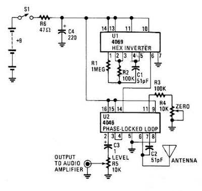
Theremin circuit shown in this schematic diagram uses digital component, so we can call it a digital Theremin. This circuit employs logic inverter 74C04 or CD4069 hex inverter and CD4046 phase-locked-loop (PLL) IC.
The CD4069 logic inverter is operated as a fixed-frequency oscillator with frequency around 100kHz. The CD4046 is operated as a variable frequency oscillator which is adjustable around 100kHz. The exact center frequency of the on-chip oscillator is determined by R4, C2 and R3. Here is the schematic diagram of the circuit.
Digital Theremin Circuit Diagram
The frequency of variable oscillator frequency circuit can be shifted several kilohertz by moving your hand approaching the antenna since the C2 and the antenna form an equivalent parallel capacitance. The frequency of the variable oscillator should be set to the same frequency of fixed oscillator when there is no hand or human body close to the antenna.
This calibration is done by adjusting the zero control R4 pot with this simple rule: If both oscillators (the fixed and the variable) are set to the same frequency then the Theremin will produce no output (silent). This Theremin circuit will start producing audible tone if you move your hand approaching the antenna since it will shift the frequency of the variable oscillator. You can play this Theremin circuit by moving your right hand around the antenna and at the same time turning the volume knob R5 with your left hand.
Saturday, October 4, 2014
Digital combination Lock using CD4013
The relay coil is activated only if the code is entered in the correct order and if there is some variation, the lock is reset. Here is the correct code is 2368.When press 2 on the flop first round (IC1A) will be activated and the value of the data (pin9) is transferred to the Q output (pin13). Since the pin 9 is based the value is "0" and therefore the pin 13 is low. For further press the digits of the code in the correct sequence is "0" leads to the Q output (pin 1) of the last flip flop (IC2b). This makes the transistor and relay energised.The automatic restoration facilities managed by the resistance R11 and capacitor positive C2.The final capacitor C2 is connected to the pin assembly flops.When filp-transistor is turned on , the capacitor C2 begins to charge as the voltage across it becomes enough top-flops are reset. This makes the lock of a fixed amount of time and then automatically locks. The delay time can be adjusted by varying the values of R11 and C2.
Thursday, October 2, 2014
Digital Volume Controller Circuit
The circuit shown here is based on the switching action of transistors.
Volume of a stereo deck can be controlled with the help of a potentiometer which changes the resistance between the output of the preamplifier and input of the amplifier. This can be done with the help of decade counter, IC.4017 and some transistors.
The input is applied at collectors and the output is taken from emitters of the transistors. Depending upon the output of IC 4017, the corresponding transistor gets saturated. Output from the emitters is taken through a coupling ” capacitor to block the DC components. When pin 4 of IC 4017 ° goes high, the corresponding transistor (T2) gets saturated and the input signal is directly fed to the output through the collector resistance-:
To start with, press switch S1. The timer IC (IC 555) will start generating pulses at equal interval of time which are fed to IC2. Depending on the output of IC 4017 the transistor is selected. When desired volume reached; release the switch.
To reset the counter, switch S2 is brought to position A. The time period of the output pulses · can be set, using the formula Td: 0.693 (R1 +2VR1 + 2R32) C1 seconds.
Digital volume controller circuit diagram:

Saturday, September 6, 2014
Batteries Charger PSU Ideal for Digital Cameras
This schema was created for digital cameras. Its known the digital cameras have considerable power consumption. For example my camera Minolta E223 requires approximately 800 mA. In practice a mains power supply or high capacity NiMH accumulators (batteries) can satisfy this demand. Batteries Charger & PSU Circuit diagram: ![]() This schema consists of two parts, charger and adapter. The transformer, rectifier bridge and buffer condensator are common. Adapter is quite simply its main part is an adjustable voltage regulator LM 317 according to usual setting. Output is a suitable for camera jack plug. Voltage can be adjusted in range 2-9 V. In the charger schema a 7805 fixed voltage regulator works as current generator assured constant current during charging. This charging current can be adjusted with the 100 /1W potentiometer in range about 50-300 mA indicated by a small current measuring instrument. From one to four batteries can be charged simultaneously. The switch must be set according to number of batteries, and charging current of batteries given by manufacturer must be adjusted. This schema doesnt measure charging time and charging condition of batteries. Manufacturers give charging time, usually 14-16 h. I solved this problem with a simply, cheap mechanical mains timer. I think its accuracy is sufficient.
This schema consists of two parts, charger and adapter. The transformer, rectifier bridge and buffer condensator are common. Adapter is quite simply its main part is an adjustable voltage regulator LM 317 according to usual setting. Output is a suitable for camera jack plug. Voltage can be adjusted in range 2-9 V. In the charger schema a 7805 fixed voltage regulator works as current generator assured constant current during charging. This charging current can be adjusted with the 100 /1W potentiometer in range about 50-300 mA indicated by a small current measuring instrument. From one to four batteries can be charged simultaneously. The switch must be set according to number of batteries, and charging current of batteries given by manufacturer must be adjusted. This schema doesnt measure charging time and charging condition of batteries. Manufacturers give charging time, usually 14-16 h. I solved this problem with a simply, cheap mechanical mains timer. I think its accuracy is sufficient.
Read More..
Sandor Dobany from Hungary
dsandor@minimail.hu
Subscribe to:
Posts (Atom)


