Showing posts with label diagram. Show all posts

Monday, November 3, 2014

FLASH LIGHT ELECTRONIC DIAGRAM


FLASH LIGHT ELECTRONIC DIAGRAM 

IC NE555 works as an astable multivibrator with variation on the frequency. With this circuit, the LED blinks every half second. How long the blink time is, can be adjusted by adjusting the value of capacitor C1. Up to 18 additional LEDs can be attached to this circuit (36 LEDs total).

Components :
Diode D1-D2 : 5mm LED
Resistor R1 : 4K7 ohm
Resistor R2 : 1k ohm
Resistor R3-R4 : 330 ohm
Variable resistor VR1 : 100k ohm
Polar capacitor C1 : 10 uF/10 V
Capacitor C2 : 0.01 uF
IC1 : NE555
6V power supply
Read More..

Saturday, November 1, 2014

9V Battery Replacement Power Supply Circuit Diagram

This circuit was originally designed to power a motorcycle intercom from the vehicle supply system. This type of intercom, which is used for communication between driver and passenger, generally requires quite a bit of power. In order to improve intelligibility there is often elaborate filtering and a compander is sometimes used as well. The disadvantage is that a battery doesn’t last very long. You could use rechargeable batteries, of course, but that is often rather laborious. It seems much more obvious to use the motorcycle power supply instead. A 9-V converter for such an application has to meet a few special requirements.

9V Battery Replacement Power Supply Circuit Diagram

9V


For one, it has to prevent interference from, for example, the ignition system reaching the attached circuit. It is also preferable that the entire circuit fits in the 9-V battery compartment. This circuit meets these requirements quite successfully and the design has nonetheless remained fairly simple. In the schematic we can recognize a filter, followed by a voltage regulator and a voltage indicator. D1, which protects the circuit against reverse polarity, is followed by an LC and an RC filter (C3/L1/L2/C1/R1/C2). This filter excludes various disturbances from the motorcycle power system.

Moreover, the design with the 78L08 and D3 ensures that the voltage regulator is operating in the linear region. The nominal system voltage of 14 V can sometimes sag to about 12 V when heavy loads such as the lights are switched on. Although the circuit is obviously suitable for all kinds of applications, we would like to mention that it has been extensively tested on a Yamaha TRX850. These tests show that the converter functions very well and that the interference suppression is excellent. 
Read More..

Friday, October 31, 2014

Stun Gun Circuit Diagram

This gadget generates substantial voltage pulses which can disrupt muscle tissues and neurological system, forcing any individual who touches it in a condition of mental bewilderment. The unit may be used again attacking beasts or dangerous intruders. Be aware that, this gadget could be prohibited in your country. It may be extremely dangerous for folks with cardiac issues, who may be using external electronic apparatus (like peacemakers), since it can deliver quite a  little RF. Dont attempt reckless behavior using this gadget, it is far from a plaything.

The proposed stun gun circuit description may be understood as follows:

The 555 IC is connected as a astable to generate rectangular waves with variable frequency and duty cycle (see the potentiometers and diode). This signal is fed to a IRF840 Mosfet (not necessary to incorporate totem transistor network, as frequency would be reduced, nonetheless the IC has adequate current potential to swiftly charge/discharge the gate).

As an alternative for the mosfet a bipolar transistor works extremely well (add a 100 ohm resistor between 555 and base of the transistor). Proper BJT could be BU406, but additionally scaled-down BJT may be ok, take into account that it should be able to cope with a minimum of 2A nonstop.

The inductive boost snubber isnt called for since the electrical power is lower which is practically completely adsorbed to charge the tank capacitor, furthermore because this gadget is battery powered we dont wish to disperse the power on a resistor, yet we need to produce the sparks.

With a snubbing system you are going to encounter decreased firing levels. Utilize A PUSHBUTTON SWITCH FOR Protection

Building the Transformer: this could be the actual tedious aspect. Because it in retailers we have to construct these. Components essential: enamel copper wire (0.20 mm or 0.125 mm), ferrite rod, LDPE sheets (0.25 mm).

Coat the ferrite rod with a application of ldpe (polyethylene, as a substitute utilize electric insulating tape) and stick it (or tape it) Position 200-250 winding on the ldpe (a lot more winding would do in case the rod is more than 1), an additional ldpe application, yet another 200-250 winding and so forth to eventually have 5-6 tiers (approx 1000-1400 turns nonetheless supplementary turns wouldnt negatively affect the functionality), then again be cautious for internal arcing that could destroy it.

Insulate it once more and set the primary winding, 15-20 turns of 1mm wire would be simply fine, an excessive amount of winding will probably lead to lesser current and reduced spike in T2 secondary on account of decreased rise period, and too few is not going to saturate the core.

Go for MKP capacitors since they have minimal ESR and ESL (these are popular in tesla coils as mmc capacitors).

The spark opening could be straightforwardly a pair of crossed (although not touching) 1 mm spaced wires. It works like a voltage regulated switch, firing when the voltage is just nice to ionize the air between them (transforming it to plasma with smaller resistance). Remember that it could be sensible do put it into a compact plastic box and stuff with oil allowing bubbles away dont employ motor oil or frying oil, rather organic mineral oil which includes zero water inside.

Stun Gun Circuit Diagram

Simple


Simple Stun Gun Circuit Diagram
Read More..

Saturday, October 25, 2014

Simple Indicator for Dynamic Limiter Schematic Diagram

The indicator described here is specifically designed for adjusting the dynamic limiter described elsewhere in this edition and checking whether the maximum level of the reference voltage (P1) needs to be modified. Her e we use a 4 -to -16 decoder IC (type 4514) to monitor the state of the four-bit up/down counter in the limiter circuit. This IC can be powered from the ±8 V supply voltages of the limiter. The limiter board has a 6-way connector (K5) that provides access to the four counter outputs and the sup-ply voltages. Connector K1 of the indicator circuit can be connected to K5 on the limiter board.
 Indicator for Dynamic Limiter Schematic

One output of the 4514 goes high for each unique 4-bit combination on its inputs, while the other outputs remain logic Low. A separate current-limiting resistor is connected in series with each LED. It was not possible to use a common cathode resistor here because most LEDs have a maximum reverse blocking voltage of only 5 V, while the supply voltage here (16 V) is a good deal higher.

The 16 LEDs ar ranged in a r ow pr ov ide a ‘fluid’ indication of the control process. You can enhance the display by using different colours for the first and last LEDs, such as red for D1 (maximum gain) and green for D16 (minimum gain), with yellow for the rest of the LEDs. While observing signals from various sources (TV set, DVD, media player, etc.), you can easily use the 16 LEDS to monitor the behaviour of the limiter and adjust the setting of potentiometer P1 in the limiter circuit. It must be set such that D16 only lights up at the maximum signal level. If this is not possible and D16 remains lit a good deal of the time regardless of the position of P1, it will be necessar y to increase the value of P1. Of course, it is also poss-ible to adjust P1 so the strongest signal source extends slightly above the control range of the limiter.

This circuit can easily be assembled on a small piece of prototyping board. The current consumption is around 4 mA. link
Read More..

Build a Solar Garden Light Circuit Diagram

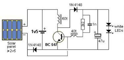
This is a Solar Garden Light Circuit Diagram that consists of a very simple system garden lighting that can be done by using some common electronic parts and a small solar panel. The electronic design is simple yet very efficient, has the advantage of being solar powered, it requires only one transistor, one 2.5 volt solar panel and some other common electronic components you can remove junk. 

This solar lighting system automatically turns on the LEDs when the solar panel detects no light turns off when the solar panel produces more than 1v and charges the battery when the panel produces more than 2.1V

The coils in this circuit require a core material F29 and they must be made with wire of 0.095 mm in core 2.6x6mm. "This circuit uses the system joule thief (joule thief) to provide voltage necessary for the LED, so other coils can be tested.

Solar Garden Light Circuit Diagram

Solar Garden Light Circuit Diagram

Read More..

Easy 2M 6M Transverter Circuit Diagram

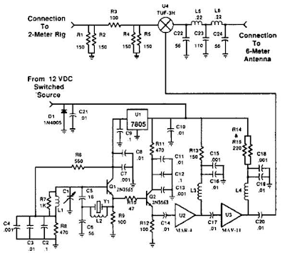
This 2M 6M Transverter Circuit Diagram Using the bilateral properties of a balanced mixer this transvertcr will produce 6-m output with 2-m inputs. Y1 is a 90-MHz crystal. Note that the input on 2 m is 143 to 144 MHz for 53 to 54-MHz output. This avoids possibility of extraneous 2-m reception during receive periods. If your radio will not transmit below 144 MHz, then use a 93- or 94-MHz crystal frequency.

2M 6M Transverter Circuit Diagram

2M 6M Transverter Circuit Diagram

Read More..

Digital Volume Control Circuit Diagram

This circuit could be used for replacing your manual volume control in a stereo amplifier. In this circuit, push-to-on switch SW1 controls the forward (volume increase) operation of both channels while a similar switch SW2 controls reverse (volume decrease) operation of both channels. A readily available IC from Dallas semiconductor, DS1669 is used here.

Circuit Diagram:


Digital Volume Control Circuit Diagram


Parts:

J1 = RCA Audio Input Socket
J2 = RCA Audio Input Socket
C1 = 0.1uF-16V Ceramic Disc Capacitor
C2 = 0.1uF-16V Ceramic Disc Capacitor
C3 = 0.1uF-16V Ceramic Disc Capacitor
IC1 = DS1669 (is available from Dallas SCo.
SW1 = Momentary Push Button Switch

Notes:
  • Replaces mechanical variable resistors.
  • Electronic interface provided for digital as well as manual control.
  • Wide differential input voltage range between 4.5 and 8 volts.
  • Wiper position is maintained in the absence of power.
  • Low-cost alternative to mechanical controls.
  • Applications include volume, tone, contrast, brightness, and dimmer control.
  • The circuit is extremely simple and compact requiring very few external components.
  • The power supply can vary from 4.5V to 8V.
  • The input signal should not fall below -0.2 volts.
Read More..

Best Automatic 12V Lead Acid Battery Charger Circuit Diagram

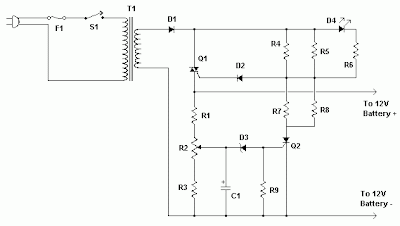
Build a Best Automatic 12V Lead Acid Battery Charger Circuit Diagram. This Best Automatic 12V Lead Acid Battery Charger Circuit Diagram will charge any 12V lead acid battery including flooded, gel and AGM. It is fully automatic and will charge at a rate up to about 4A until the battery voltage reaches a preset point at which it will switch to a very low current float charge. 

If the battery voltage drops again the charger will begin charging until the voltage once again reaches the cut off point. In this way it can be left connected to a battery indefinitely to maintain full charge without causing damage. An LED indicates when the battery is fully charged. Sourced By Circuitsstream

Best Automatic 12V Lead Acid Battery Charger Circuit Diagram

Best Automatic 12V Lead Acid Battery Charger Circuit Diagram

 Commponents


Part

Total Qty.

Description

Substitutions
R1, R32330 Ohm 1/4W Resistor
R21100 Ohm 1/4W Pot
R4, R5, R7, R8482 Ohm 2W Resistor
R61100 Ohm 1/4W Resistor
R911K 1/4W Resistor
C11220uF 25V Electrolytic Capacitor
D11P600 DiodeAny 50V 5A or greater rectifier diode
D211N4004 Diode1N4002, 1N4007
D315.6V Zener Diode
D41LED (Red, Green or Yellow)
Q11BT136 TRIAC
Q21BRX49 SCR
T1112V 4A TransformerSee Notes
F113A Fuse
S11SPST Switch, 120VAC 5A
MISC1Wire, Board, Heatsink For U1, Case, Binding Posts or Alligator Clips For Output, Fuse Holder

Notes 

R2 will have to be adjusted to set the proper finish charge voltage. Flooded and gel batteries are generally charged to 13.8V. If you are cycling the battery (AGM or gel) then 14.5V to 14.9V is generally recommended by battery manufacturers. To set up the charger, set the pot to midway, turn on the charger and then connect a battery to its output. Monitor the charge with a voltmeter until the battery reaches the proper end voltage and then adjust the pot until the LED glows steadily. The charger has now been set. To charge multiple battery types you can mount the pot on the front of the case and have each position marked for the appropriate voltage.

Q1 will need a heatsink. If the circuit is mounted in a case then a small fan might be necessary and can generally be powered right off the output of D1.

T1 is a transformer with a primary voltage appropriate to your location (120V, 220V, etc.) and a secondary around 12V. Using a higher voltage secondary (16V-18V) will allow you to charge 16V batteries sometimes used in racing applications.

If the circuit is powered off, the battery should be disconnected from its output otherwise the circuit will drain the battery slowly.
Read More..

25 Watt Audio Amplifier Circuits Diagram

25 Watt Audio Amplifier Circuits Diagram

25 Watt Audio Amplifier Circuits Diagram

Parts:

R1,R4_________47K  1/4W Resistors
R2____________4K7  1/4W Resistor
R3____________1K5  1/4W Resistor
R5__________390R   1/4W Resistor
R6__________470R   1/4W Resistor
R7___________33K   1/4W Resistor
R8__________150K   1/4W Resistor
R9___________15K   1/4W Resistor
R10__________27R   1/4W Resistor
R11_________500R   1/2W Trimmer Cermet
R12,R13,R16__10R   1/4W Resistors
R14,R15_____220R   1/4W Resistors
R17___________8R2    2W Resistor
R18____________R22   4W Resistor (wirewound)
 
C1___________470nF  63V Polyester Capacitor
C2___________330pF  63V Polystyrene Capacitor
C3,C5________470µF  63V Electrolytic Capacitors
C4,C6,C8,C11_100nF  63V Polyester Capacitors
C7___________100µF  25V Electrolytic Capacitor
C9____________10pF  63V Polystyrene Capacitor
C10____________1µF  63V Polyester Capacitor
 
Q1-Q5______BC560C   45V 100mA Low noise High gain PNP Transistors
Q6_________BD140    80V 1.5A PNP Transistor
Q7_________BD139    80V 1.5A NPN Transistor
Q8_________IRF530  100V 14A N-Channel Hexfet Transistor
Q9_________IRF9530 100V 12A P-Channel Hexfet Transistor
 

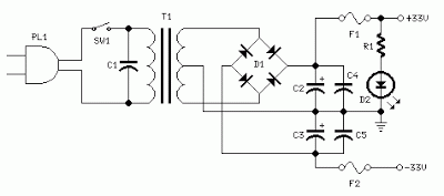
Power supply circuit diagram


Power supply circuit diagram


Parts:

R1____________3K3  1/2W Resistor C1___________10nF 1000V Polyester CapacitorC2,C3______4700µF   50V Electrolytic CapacitorsC4,C5_______100nF   63V Polyester Capacitors D1__________200V 8A Diode bridgeD2__________5mm. Red LED F1,F2_______3.15A Fuses with sockets T1__________220V Primary, 25 + 25V Secondary 120VA Mains transformer PL1_________Male Mains plug SW1_________SPST Mains switch
 

Notes:

  • Can be directly connected to CD players, tuners and tape recorders. Simply add a 10K Log potentiometer (dual gang for stereo) and a switch to cope with the various sources you need.
  • Q6 & Q7 must have a small U-shaped heatsink.
  • Q8 & Q9 must be mounted on heatsink.
  • Adjust R11 to set quiescent current at 100mA (best measured with an Avo-meter connected in series to Q8 Drain) with no input signal.
  • A correct grounding is very important to eliminate hum and ground loops. Connect to the same point the ground sides of R1, R4, R9, C3 to C8. Connect C11 to output ground. Then connect separately the input and output grounds to power supply ground.
  • An earlier prototype of this amplifier was recently inspected and tested again after 15 years of use.

Technical data:

Output power:
well in excess of 25 Watt RMS @ 8 Ohm (1KHz sine wave)
Sensitivity:
200mV input for 25W output
Frequency response:
30Hz to 20KHz-1dB
Total harmonic distortion @ 1KHz:
0.1W 0.014% 1W 0.006% 10W 0.006% 20W0.007% 25W 0.01%
Total harmonic distortion @10KHz:
0.1W 0.024% 1W 0.016% 10W 0.02% 20W0.045% 25W 0.07%
Unconditionally stable on capacitive loads
Read More..

Friday, October 24, 2014

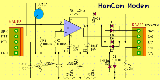
Modem for Digital Modes Circuits Diagram

Ham Com is a modem for almost all types of digital transmission for radio amateurs. It can be used to RTTY, ASCII, NevTex, Sitor, Amtor, Fec, CW, FSK, etc.. The modem is simple and can even be used for receiving faxes and SSTV wx-using JV-FAX software.

 Modem for Digital Modes Circuits Diagram

Modem for Digital Modes Circuits Diagram


To use this modem, you need a PC with serial port, Software HamCom and radio equipment.
Read More..

25 Watt Audio Amplifier Circuits Diagram

25 Watt Audio Amplifier Circuits Diagram

25 Watt Audio Amplifier Circuits Diagram

Parts:

R1,R4_________47K  1/4W Resistors
R2____________4K7  1/4W Resistor
R3____________1K5  1/4W Resistor
R5__________390R   1/4W Resistor
R6__________470R   1/4W Resistor
R7___________33K   1/4W Resistor
R8__________150K   1/4W Resistor
R9___________15K   1/4W Resistor
R10__________27R   1/4W Resistor
R11_________500R   1/2W Trimmer Cermet
R12,R13,R16__10R   1/4W Resistors
R14,R15_____220R   1/4W Resistors
R17___________8R2    2W Resistor
R18____________R22   4W Resistor (wirewound)
 
C1___________470nF  63V Polyester Capacitor
C2___________330pF  63V Polystyrene Capacitor
C3,C5________470µF  63V Electrolytic Capacitors
C4,C6,C8,C11_100nF  63V Polyester Capacitors
C7___________100µF  25V Electrolytic Capacitor
C9____________10pF  63V Polystyrene Capacitor
C10____________1µF  63V Polyester Capacitor
 
Q1-Q5______BC560C   45V 100mA Low noise High gain PNP Transistors
Q6_________BD140    80V 1.5A PNP Transistor
Q7_________BD139    80V 1.5A NPN Transistor
Q8_________IRF530  100V 14A N-Channel Hexfet Transistor
Q9_________IRF9530 100V 12A P-Channel Hexfet Transistor
 

Power supply circuit diagram


Power supply circuit diagram


Parts:

R1____________3K3  1/2W Resistor C1___________10nF 1000V Polyester CapacitorC2,C3______4700µF   50V Electrolytic CapacitorsC4,C5_______100nF   63V Polyester Capacitors D1__________200V 8A Diode bridgeD2__________5mm. Red LED F1,F2_______3.15A Fuses with sockets T1__________220V Primary, 25 + 25V Secondary 120VA Mains transformer PL1_________Male Mains plug SW1_________SPST Mains switch
 

Notes:

  • Can be directly connected to CD players, tuners and tape recorders. Simply add a 10K Log potentiometer (dual gang for stereo) and a switch to cope with the various sources you need.
  • Q6 & Q7 must have a small U-shaped heatsink.
  • Q8 & Q9 must be mounted on heatsink.
  • Adjust R11 to set quiescent current at 100mA (best measured with an Avo-meter connected in series to Q8 Drain) with no input signal.
  • A correct grounding is very important to eliminate hum and ground loops. Connect to the same point the ground sides of R1, R4, R9, C3 to C8. Connect C11 to output ground. Then connect separately the input and output grounds to power supply ground.
  • An earlier prototype of this amplifier was recently inspected and tested again after 15 years of use.

Technical data:

Output power:
well in excess of 25 Watt RMS @ 8 Ohm (1KHz sine wave)
Sensitivity:
200mV input for 25W output
Frequency response:
30Hz to 20KHz-1dB
Total harmonic distortion @ 1KHz:
0.1W 0.014% 1W 0.006% 10W 0.006% 20W0.007% 25W 0.01%
Total harmonic distortion @10KHz:
0.1W 0.024% 1W 0.016% 10W 0.02% 20W0.045% 25W 0.07%
Unconditionally stable on capacitive loads
Read More..

Smart Chocolate Block Schematic Diagram

What can be done, when two light bulbs in one light fitting are to be switched separately, but only one switch circuit is available? Simple: build a ‘smart chocolate block’ into the ceiling rose! The circuit is built from discrete components and with a bit of ingenuity can be fitted onto a printed circuit board measuring just a centimetre or two square.

When light switch S1 is operated for the first time lamp La1, which is connected in the usual way, lights; La2 remains dark. Electrolytic capacitor C1 starts to charge via rectifier diode D1 and resistors R1 and R2 until zener diode D3 conducts, limiting the voltage to about 6.8 V. This voltage is used as a supply for the rest of the circuit. The second lamp is connected via a triac and a fuse (1.5 A, medium speed recommended). The triac is triggered by T4, which can only happen when T3 does not pull its base down to ground. The first time the circuit is switched on this is the case, as we shall see below.
Smart Chocolate Block Schematic
Smart Chocolate Block Circuit Schematic Diagram
Transistors T1 and T2 form a bistable flip-flop with a well-defined power-up state. R14 and R15 cause both transistors to be initially turned off. As the voltage across C1 rises, transistor T1, driven via resistors R7 and R9, turns on. The base drive for transistor T2, which is provided via D2, the low-pass filter formed by R6 and C2, and R5, would arrive a little later, but when T1 turns on it diverts the base current away from T2, which therefore remains turned off. This situation is stable: the base of T3 is not pulled down and so this transistor conducts.

To turn the second lamp on, switch S1 is opened and then, within a second or so, closed again. The effect of this action on the flip-flop is as follows.

When the switch is opened the voltage across C1 falls more rapidly than the volt-age across C2. The main reason for this is resistor R3, which is directly responsible for the discharge of C1; C2 can only discharge through the relatively high resistance of R5, since the other path is blocked by diode D2. This means that T2 is driven via R5 for one or two seconds longer than T1 is driven via R7 and R9. If during this time the supply voltage reappears, it can no longer drive the base of T1 via R7 as T2 is conducting all the current to ground. This situation is also stable, as C2 is recharged via D2 and R6.

When T2 conducts it pulls the base of T3 to ground, so that this latter transistor turns off. Darlington transistor T4 now conducts as its base is pulled high via R4. T4 now provides the trigger current for the triac via current limiting resistor R10, and the second lamp lights.

T5 and T6 together form a zero-crossing detector. It ensures that the triac is never triggered at a moment when the AC mains supply is at a high voltage point in its cycle. This avoids a rapid inrush current into La2, which would give rise to considerable radio interference. Also, trigger current is only required for the triac for a small fraction of the period of one cycle of the mains supply. If this current were drawn continuously from the low voltage supply, C1 would rap-idly discharge; R1 and R2 would have to be considerably reduced in resistance, which would increase the heat dissipation of the module, perhaps making it infeasible to build the circuit into a plastic ceiling rose.

Using the component values shown the triac is only driven when the instantaneous mains voltage is less than about 15 V in magnitude. The voltage divider formed by R11, R12 and R13 switches on the transistors T5 and T6 when the voltage is greater than +15V or less than –15 V respectively. The collectors of these transistors, which are connected together, pull the base of T4 down to ground or to a slightly negative voltage when the mains cycle is outside the desired phase window.

Any resistors across which mains voltages will be dropped are formed from two individual resistors wired in series to ensure that the maximum voltage specifications of ordinary 0.25 W components are not exceeded. This applies to R1 and R2, as well as R11 and R12. The whole circuit is at mains potentials and great care must be taken to observe all relevant safety precautions in construction and installation. link
Read More..

Simple Color Organ Circuit Diagram

Three Lamp-Channels Output Built-in Electret Microphone
A simple, satisfactory Color Organ can be built with a handful of cheap components. This design features: no mains supply transformer, built-in microphone and three widely adjustable frequency bands obtained by means of very simple, passive filters for Bass, Middle and Treble.

Circuit diagram :
Simple Color Organ-Circuit Diagram
Simple Color Organ Circuit Diagram
Due to the very low current consumption of this circuit, the mains supply can be conveniently reduced with no heat dissipation by the reactance of C1; then rectified by D1 and D2 and clamped to 24V by the Zener Diode D3. The music diffused by the loudspeaker(s) of any type of media player, is picked-up by the built-in microphone and the resulting signal is greatly amplified by a two-stage transistor audio amplifier Q1 and Q2.
At the output of the second stage, the audio signal is filtered and split into three fully adjustable frequency bands by means of a simple (though effective) passive filter formed by P1, P2, P3, R7, R8, C6 and C7, thus avoiding the complexity of op-amp based active filters. Transistors Q3, Q4 and Q5 are the drivers for the Triacs D4, D5 and D6 respectively, but can be omitted if high sensitivity Triac devices are used.
Parts:
P1,P2,P3_____10K   Linear Potentiometers
R1_____470R   1/2W Resistor
R2_____100K   1/4W Resistor
R3_____1M   1/4W Resistor
R4_____22K   1/4W Resistor
R5_____220K   1/4W Resistor
R6_____15K   1/4W Resistor
R7_____1K5  1/4W Resistor
R8_____4K7  1/4W Resistor
C1_____330nF  400V Polyester Capacitor
C2_____470µF   35V Electrolytic Capacitor
C3,C4,C6_____100nF   63V Polyester or Ceramic Capacitors
C5_____1µF   63V Electrolytic Capacitor
C7_____4n7   63V Polyester or Ceramic Capacitor
D1,D2_____1N4007 1000V 1A Diodes
D3_____BZX79C24   24V 500mW Zener Diode
D4,D5,D6_____TIC206M  600V 4A TRIACs
Q1 to Q5_____BC547   45V 100mA NPN Transistors
MIC1_____Miniature Electret Microphone Capsule
SW1_____SPST Toggle Switch 250V 10-15A (See Notes)
PL1_____Male Mains Plug
SK1,SK2,SK3_____Female Mains Sockets
Notes :
  • sing the Triac types suggested in the Parts List, each channel can drive several incandescent lamp bulbs, up to about 800W, but in this case a separate heatsink must be used for each Triac.
  • Due to the absence of a mains transformer, avoid to connect this circuit to other appliances (e.g. to the output of an amplifier by means of a cable). Please use only the microphone enclosed into the main case to pick-up the music.
  • For 110-120V mains operation, C1 value must be doubled: use two 330nF capacitors wired in parallel or one 680nF 250V capacitor. No further modification is required.
  • SW1 must be a high voltage, high current switch, as it must withstand the total amount of current drawn by all bulbs wired to the three outputs of the circuit.
Warning! The device is connected to 230Vac mains, then some parts in the circuit board are subjected to lethal potential! Avoid touching the circuit when plugged and enclose it in a plastic or wooden box.


Read More..

Converter RS232 to Arduino Circuit Diagram

 Converter RS232 to Arduino Circuit Diagram

The circuit in this article is an RS232 converter, it is possible to connect an Arduino bootloader or your chip with a RS232 port. Here are two versions, one very simple and functional above and one below a little more sophisticated. The port 232 gives a bit more work than USB, but in case of equipment that only have this feature that is a good outlet.

 Converter RS232 to Arduino Circuit Diagram

 Converter RS232 to Arduino Circuit Diagram

Read More..

Automatic Range Switching Circuit Diagram

You can pick up a 3½-digit digital volt-meter module nowadays for a little as a couple quid. This is a simple and expensive way to fit out a piece of equipment with an instrument. Most modules are based on the well-known ICL7106 IC . They operate from an ordinary 9-V battery, and they only provide a fixed measuring range (200 mV or 2 V). The accessory circuit described here converts a DVM module into a voltmeter with 20-V and 200-V measuring ranges, with the added bonus of automatic range switching.

This requires a ground-referenced symmetrical supply voltage (±5 V) instead of a battery. An inexpensive TL431C is also used to generate an adjustable reference volt-age from the supply voltage. The circuit described here uses an LCD module with a fixed measuring range of 200 mV. It has three pins for driving the decimal point; two of them are used here.

Automatic Range Switching Schematic

Switches Schematic

This is how the circuit works: IC1 converts the voltage to be measured by the DVM module into a ground-referenced voltage. This part of the circuit is based on a design idea from Carsten Weber [1] that was pub-lished in the June 2005 issue of Elektor Electronics.

If the input voltage is less than 20 V, the voltage divider formed by R1 and R4 reduces it by a factor of 100. Transistor T2 is cut off, so R3 has no effect on the division ratio. The voltage at the junction of voltage divider R8/R13 is 200 mV because the open-collector output of comparator IC2A is in the high-impedance state. If the input voltage rises above 20 V, IC2A changes state and the voltage at the junction of voltage divider R8/R13 drops to less than 20 mV. In response to this, the out-put of comparator IC2B goes high and T2 conducts. R3 is now connected in parallel with R4.

This yields a division factor of 1000 (200-V range). Of course, the larger division factor also causes the input voltage of IC2A to drop. To prevent this comparator from changing back to its previous state (which would cause the circuit to act like a sort of oscillator), the value of R10 must be chosen such that the voltage at the junction of voltage divider R8/R13 is less than 20 mV, as previously mentioned. The calculated value (with R10 in parallel with R13) is approximately 9.6 mV. In practice, the value is around 18 mV due to the resistance of the output transistor of the comparator.

This means that the circuit will switch back to the lower voltage range when the input voltage drops below approximately 18 V. The amount of hysteresis can be set by adjusting the value of R10. However, the circuit will oscillate if the value is too high. Film capacitors C1, C3 and C4 sup-press noise and create a certain amount of inertia for range switching. This prevents frequent back-and-forth switching in the threshold region.

The other two comparators of IC2 sup-ply mutually complementary output levels that depend on the measuring range. The associated decimal points of the DVM module are driven via p-channel FETs.The circuit has two trimpots: P1 is used to correct for the offset voltage of the operational amplifier (IC1), while P2 is used to set the threshold level for range switching For this purpose, first adjust the trimpot to produce the maximum possible reference voltage (around 3.4 V). Next apply an input voltage that causes a display reading of 19.99 (which ideally means 19.99 V). Now turn P2 until the measuring range switches.

As a check, reduce the input voltage to force the measuring range to switch back, and then slowly increase the input voltage again. The ideal setting is reached when the measuring range switches before the DVM module displays an ‘overrange’ indication. Link


Author : Rainer Reusch - Copyright: Elektor
Read More..

Build a Wire Break Alarm With Delay Circuit Diagram

Here is a simple circuit of wire-break alarm that activates after a delay of 15 to 30 seconds. When the thin-wire loop running across the entrance door is broken, the alarm sounds after a delay of 15 to 30 seconds, the time period set through VR1. Thus the occupants get sufficient time to lock the room from the outside and catch the thief. 

The circuit uses CD4060, which is a 14-stage ripple-carry binary counter/divider and oscillator. It is wired as a timer here and does not need input pulse for trigger. CD4060 gets activated as soon as the power supply is switched on. Output O13 of CD4060 goes high after the lapse of preset delay set through VR1. Transistor SL100 (T2) is wired as a switch to power the timer section built around CD4060. When the wire loop is closed, transistor T2 does not conduct. So power to the timer circuit is not available and the piezobuzzer does not sound. 

Wire-Break Alarm With Delay Circuit Schematic

Build a Wire-Break Alarm With Delay Circuit Diagram

On the other hand, when the wire loop is broken by some intruder, transistor T2 conducts to power the circuit and the piezobuzzer sounds after 15 to 30 seconds. IC1 can be reset by connecting the wire loop or interrupting the supply. The circuit works off regulated 9V-12V. Assemble it on a general-purpose PCB and enclose in a metallic or plastic box of appropriate size. Connect piezobuzzer PZ1 through external wires and complete the installation.
Read More..

Thursday, October 23, 2014

BFO Metal detectors Circuit Diagram

This metal detector circuit consists of two oscillators, both working at about 465 kHz. One uses a transformer and the other uses an inductor which is the search coil LI. The oscillators are coupled through a capacitor 10 pF. The circuits DE metal detector is a BFO (beat frequency oscillator), a tone beat produced if the two oscillators are working together through the diode is detected and sent to the audio amplifier. 

 BFO Metal detectors Circuit Diagram

BFO Metal detectors Circuit Diagram


The oscillator coil is tuned by a variable capacitor of 10-365 pf variable. The search coil is made of wire with 22 turns between 24 and 36 AWG enamel junction to the center. The wire should be wound on a form of about 6 "χ 6" and the phones must be high impedance.
Read More..

Build a 18W Audio Amplifier Circuits Diagram

18W Audio Amplifier Circuits Diagram

Amplifier parts:

P1_____________22K  Log. Potentiometer (Dual-gang for stereo)
 
R1______________1K  1/4W Resistor
R2______________4K7 1/4W Resistor
R3____________100R  1/4W Resistor
R4______________4K7 1/4W Resistor
R5_____________82K  1/4W Resistor
R6_____________10R  1/2W Resistor
R7_______________R22  4W Resistor (wirewound)
R8______________1K  1/2W Trimmer Cermet (optional)
 
C1____________470nF  63V Polyester Capacitor
C2,C5_________100µF   3V Tantalum bead Capacitors
C3,C4_________470µF  25V Electrolytic Capacitors
C6____________100nF  63V Polyester Capacitor
 
D1___________1N4148  75V 150mA Diode
 
IC1________TLE2141C  Low noise, high voltage, high slew-rate Op-amp
 
Q1____________BC182  50V 100mA NPN Transistor
Q2____________BC212  50V 100mA PNP Transistor
Q3___________TIP42A  60V 6A    PNP Transistor
Q4___________TIP41A  60V 6A    NPN Transistor
 
J1______________RCA  audio input socket

Power supply parts:

R9______________2K2 1/4W Resistor
 
C7,C8________4700µF 25V Electrolytic Capacitors
 
D2_____________100V 4A Diode bridge
D3_____________5mm. Red LED
 
T1_____________220V Primary, 15 + 15V Secondary, 50VA Mains transformer
 
PL1____________Male Mains plug
 
SW1____________SPST Mains switch


Notes:

  • Can be directly connected to CD players, tuners and tape recorders.
  • Do not exceed 23 + 23V supply.
  • Q3 and Q4 must be mounted on heatsink.
  • D1 must be in thermal contact with Q1.
  • Quiescent current (best measured with an Avo-meter in series with Q3 Emitter) is not critical.
  • Adjust R3 to read a current between 20 to 30 mA with no input signal.
  • To facilitate quiescent current setting add R8 (optional).
  • A correct grounding is very important to eliminate hum and ground loops. Connect to the same point the ground sides of J1, P1, C2, C3 & C4. Connect C6 to the output ground.
  • Then connect separately the input and output grounds to the power supply ground. 
 Technical data:
Output power:
18 Watt RMS into 8 Ohm (1KHz sine wave)
Sensitivity:
150mV input for 18W output
Frequency response:
30Hz to 20KHz-1dB
Total harmonic distortion @ 1KHz:
0.1W 0.02% 1W 0.01% 5W 0.01% 10W0.03%
Total harmonic distortion @10KHz:
0.1W 0.04% 1W 0.05% 5W 0.06% 10W0.15%
Unconditionally stable on capacitive loads
Read More..

Simple and hold circuit using op amp Circuits Diagram

As the name indicates , a sample and hold circuit is a circuit which samples an input signal and holds onto its last sampled value until the input is sampled again. Sample and hold circuits are commonly used in analogue to digital converts, communication circuits, PWM circuits etc. The circuit shown below is of a sample and hold circuit based on uA 741 opamp , n-channel E MOSFET BS170 and few passive components.

Description

As the name indicates , a sample and hold circuit is a circuit which samples an input signal and holds onto its last sampled value until the input is sampled again. Sample and hold circuits are commonly used in analogue to digital converts, communication circuits, PWM circuits etc. The circuit shown below is of a sample and hold circuit based on uA 741 opamp , n-channel E MOSFET BS170 and few passive components.

In the circuit MOSFET BS170 (Q1) works as a switch while opamp uA741 is wired as a voltage follower. The signal to be sampled (Vin) is applied to the drain of MOSFET while the sample and hold control voltage (Vs) is applied to the source of the MOSFET. The source pin of the MOSFET is connected to the non inverting input of the opamp through the resistor R3. C1 which is a polyester capacitor serves as the charge storing device. Resistor R2 serves as the load resistor while preset R1 is used for adjusting the offset voltage.
During the positive half cycle of the Vs, the MOSFET is ON which acts like a closed switch and the capacitor C1 is charged by the Vin and the same voltage (Vin) appears at the output of the opamp. When Vs is zero MOSFET is switched off and the only discharge path for C1 is through the inverting input of the opamp. Since the input impedance of the opamp is too high the voltage Vin is retained and it appears at the output of the opamp.

The time periods of the Vs during which the voltage across the capacitor (Vc) is equal to Vin are called sample periods (Ts) and the time periods of Vs during which the voltage across the capacitor C1 (Vc) is held constant are called hold periods (Th). Taking a close look at the input and output wave forms of the circuit will make it easier to understand the working of the circuit.

Circuit diagram

 Sample and Hold circuit using uA741 opamp

Input and output waveforms.

sample and hold waveforms
Input and output waveforms - Sample and hold circuit

Notes

  • The circuit can be assembled on a vero board.
  • Use +15V/-15V DC dual supply for powering the opamp.
  • Capacitor C1 must have minimum leakage current possible and thats why a polyester capacitor is used here.
  • Mount the IC uA741 on a holder.
  • The type number of the MOSFET Q1 is not very significant here and so substitution is possible if BS170 is not available.
  • BS170 is a 60V, 500mA n-channel enhancement mode MOSFET available in TO-92 package.
  • Preset resistor R1 can be used for offset adjustments.
Read More..

Simple Regenerative Receiver Circuit Diagram 80m or 40m

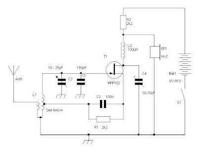
This is a simple design, can have excellent results, he is a recipient of regeneration, if you have never built any receiver, this is one you will build Easy. The circuit described is simple and has many limitations in sensitivity and selectivity, but is able to receive signals from radio amateurs (40m or 80m) in SSB and CW, and as output using a small headset crystal. 

He will have a saturation if there are strong stations available on AM broadcast band of 41m at night.L1 is a small toroid T50-2 (red) with about 18 to 20 times (40m) or 35 to 40 times (80m) in the main winding connected to the FET with a single coupling circuit facing the antenna connection. 

The center tap is about 20% of the primary winding. C1 is adjusted to set the radio band to the 40m and C2 then acts as a fine tuning within the band.The supply of 12 to 14V, R2 should be increased 5K6 or 6K8 output will be higher and similar sensitivity to-100dBm (about 2uV).

Regenerative Receiver Circuit Diagram

Regenerative Receiver Circuit Diagram

Read More..