Showing posts with label a. Show all posts

Saturday, October 25, 2014

Build a Solar Garden Light Circuit Diagram

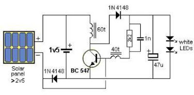
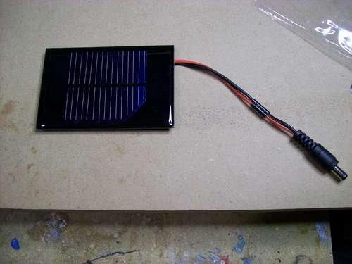
This is a Solar Garden Light Circuit Diagram that consists of a very simple system garden lighting that can be done by using some common electronic parts and a small solar panel. The electronic design is simple yet very efficient, has the advantage of being solar powered, it requires only one transistor, one 2.5 volt solar panel and some other common electronic components you can remove junk. 

This solar lighting system automatically turns on the LEDs when the solar panel detects no light turns off when the solar panel produces more than 1v and charges the battery when the panel produces more than 2.1V

The coils in this circuit require a core material F29 and they must be made with wire of 0.095 mm in core 2.6x6mm. "This circuit uses the system joule thief (joule thief) to provide voltage necessary for the LED, so other coils can be tested.

Solar Garden Light Circuit Diagram

Solar Garden Light Circuit Diagram

Read More..

Friday, October 24, 2014

Build a Wire Break Alarm With Delay Circuit Diagram

Here is a simple circuit of wire-break alarm that activates after a delay of 15 to 30 seconds. When the thin-wire loop running across the entrance door is broken, the alarm sounds after a delay of 15 to 30 seconds, the time period set through VR1. Thus the occupants get sufficient time to lock the room from the outside and catch the thief. 

The circuit uses CD4060, which is a 14-stage ripple-carry binary counter/divider and oscillator. It is wired as a timer here and does not need input pulse for trigger. CD4060 gets activated as soon as the power supply is switched on. Output O13 of CD4060 goes high after the lapse of preset delay set through VR1. Transistor SL100 (T2) is wired as a switch to power the timer section built around CD4060. When the wire loop is closed, transistor T2 does not conduct. So power to the timer circuit is not available and the piezobuzzer does not sound. 

Wire-Break Alarm With Delay Circuit Schematic

Build a Wire-Break Alarm With Delay Circuit Diagram

On the other hand, when the wire loop is broken by some intruder, transistor T2 conducts to power the circuit and the piezobuzzer sounds after 15 to 30 seconds. IC1 can be reset by connecting the wire loop or interrupting the supply. The circuit works off regulated 9V-12V. Assemble it on a general-purpose PCB and enclose in a metallic or plastic box of appropriate size. Connect piezobuzzer PZ1 through external wires and complete the installation.
Read More..

Thursday, October 23, 2014

Build a 18W Audio Amplifier Circuits Diagram

18W Audio Amplifier Circuits Diagram

Amplifier parts:

P1_____________22K  Log. Potentiometer (Dual-gang for stereo)
 
R1______________1K  1/4W Resistor
R2______________4K7 1/4W Resistor
R3____________100R  1/4W Resistor
R4______________4K7 1/4W Resistor
R5_____________82K  1/4W Resistor
R6_____________10R  1/2W Resistor
R7_______________R22  4W Resistor (wirewound)
R8______________1K  1/2W Trimmer Cermet (optional)
 
C1____________470nF  63V Polyester Capacitor
C2,C5_________100µF   3V Tantalum bead Capacitors
C3,C4_________470µF  25V Electrolytic Capacitors
C6____________100nF  63V Polyester Capacitor
 
D1___________1N4148  75V 150mA Diode
 
IC1________TLE2141C  Low noise, high voltage, high slew-rate Op-amp
 
Q1____________BC182  50V 100mA NPN Transistor
Q2____________BC212  50V 100mA PNP Transistor
Q3___________TIP42A  60V 6A    PNP Transistor
Q4___________TIP41A  60V 6A    NPN Transistor
 
J1______________RCA  audio input socket

Power supply parts:

R9______________2K2 1/4W Resistor
 
C7,C8________4700µF 25V Electrolytic Capacitors
 
D2_____________100V 4A Diode bridge
D3_____________5mm. Red LED
 
T1_____________220V Primary, 15 + 15V Secondary, 50VA Mains transformer
 
PL1____________Male Mains plug
 
SW1____________SPST Mains switch


Notes:

  • Can be directly connected to CD players, tuners and tape recorders.
  • Do not exceed 23 + 23V supply.
  • Q3 and Q4 must be mounted on heatsink.
  • D1 must be in thermal contact with Q1.
  • Quiescent current (best measured with an Avo-meter in series with Q3 Emitter) is not critical.
  • Adjust R3 to read a current between 20 to 30 mA with no input signal.
  • To facilitate quiescent current setting add R8 (optional).
  • A correct grounding is very important to eliminate hum and ground loops. Connect to the same point the ground sides of J1, P1, C2, C3 & C4. Connect C6 to the output ground.
  • Then connect separately the input and output grounds to the power supply ground. 
 Technical data:
Output power:
18 Watt RMS into 8 Ohm (1KHz sine wave)
Sensitivity:
150mV input for 18W output
Frequency response:
30Hz to 20KHz-1dB
Total harmonic distortion @ 1KHz:
0.1W 0.02% 1W 0.01% 5W 0.01% 10W0.03%
Total harmonic distortion @10KHz:
0.1W 0.04% 1W 0.05% 5W 0.06% 10W0.15%
Unconditionally stable on capacitive loads
Read More..

Making a Solar Energy Powered an iPhone Battery Charger

The project was termed as Mighty Minty Boost as it was developed to function as iPod/iPhone charger with solar power. Aside from being small, it has a large battery capacity of 3.7V at 2000mAh and it accepts input power from 3.7V to 7V. As shown in the images below, it can become a compact USB power supply when the solar cell is removed after charging. The Velcro is used to secure the Mighty Minty Boost inside a backpack or messenger bag after unplugging the solar cell.

For faster charging, a larger solar cell can be attached to the bag. Enough power can be generated to fully charge an iPhone in about 5.5 hours and an iPod Touch in 4 hours using a slightly larger solar cell with 6V at 250mAh. The charger will automatically switch to trickle charging when the cell reaches full charge. The charging current is limited to 100mA when charging using the mini USB port and the charging is limited to 280mA when charging using the barrel plug jack

Hacks and Mods: iPhone Charger Powered Thru Solar Energy
.
The materials needed to build the charger include a small solar cell, Lithium Polymer battery charger, minty boost kit, adhesive backed Velcro, Altoids tin, connector/wire, and small double adhesive squares as shown in the images below. An input power that ranges from 3.7V to 7V maximum can be accepted by the single cell Lithium Polymer. In bright sunlight, the solar cell maxes out at approximately 5V at 100mA. A larger solar cell with 6V at 250mA can be used for faster charging.

Hacks and Mods: iPhone Charger Powered Thru Solar Energy

The images below show the assembly of minty boost kit where a JST connector is soldered to the minty boost PCB instead of connecting the battery holder in the kit. The minty boost circuit is allowed to connect to the Lithium Polymer battery charger circuit with this tiny connector. The minty boost is tested by connecting the battery pack and the charger circuit, the Lithium Polymer battery connects to the connector marked GND on the charger board and the minty boost connects to the connector marked SYS.

Hacks and Mods: iPhone Charger Powered Thru Solar Energy

To fit the charger, a notch is cut out of the other side of the Altoids tin and used double sided adhesive to secure the charging circuit to the bottom of the Altoids as shown below. The bottom of either one of the circuit boards should not touch the bottom of the Altoids tin while reconnecting the minty boost PCB and the battery to the charging circuit.

Hacks and Mods: iPhone Charger Powered Thru Solar Energy

Connecting or adding the solar cell can be done in different ways. Shortening the connector leads and plugging the barrel plug into the barrel jack on the charging circuit is one way. The other method is using another JST connector to replace the connector and plugging it into the third connector marked 5V on the charging circuit. Since there is no bog barrel plug sticking out of the side of the tin, using the second method is cleaner.

As shown in the photos below, some 2” Velcro was used to attach the solar cell to the top of the Altoids. To help protect the battery, a layer of clear packing tape was used for wrapping. N top of the two circuit boards, the battery pack is then set down. A red LED on the charger board will light up when the Mighty Minty Boost is set out in the bright sun. The iPod/iPhone/USB powered device can be connected once it is fully charged.

Hacks and Mods: iPhone Charger Powered Thru Solar Energy
Read More..

Monday, October 20, 2014

Converting a DCM Motor

We recently bought a train set made by a renowned company and just couldn’t resist looking inside the locomotive. Although it did have an electronic decoder, the DCM motor was already available 35 (!) years ago. It is most likely that this motor is used due to financial constraints, because Märklin (as you probably guessed) also has a modern 5-pole motor as part of its range. Incidentally, they have recently introduced a brushless model. 

The DCM motor used in our locomotive is still an old-fashioned 3-pole series motor with an electromagnet to provide motive power. The new 5-pole motor has a permanent magnet. We therefore wondered if we couldn’t improve the driving characteristics if we powered the field winding separately, using a bridge rectifier and a 27 Ω current limiting resistor. This would effectively create a permanent magnet. The result was that the driving characteristics improved at lower speeds, but the initial acceleration remained the same. But a constant 0.5 A flows through the winding, which seems wasteful of the (limited) track power. A small circuit can reduce this current to less than half, making this technique more acceptable. 

Circuit diagram :
Converting a DCM Motor-Circuit Diagram
Converting a DCM Motor Circuit Diagram

The field winding has to be disconnected from the rest (3 wires). A freewheeling diode (D1, Schottky) is then connected across the whole winding. The centre tap of the winding is no longer used. When FET T1 turns on, the current through the winding increases from zero until it reaches about 0.5 A. At this current the voltage drop across R4-R7 becomes greater than the reference voltage across D2 and the opamp will turn off the FET. The current through the winding continues flowing via D1, gradually reducing in strength. When the current has fallen about 10% (due to hysteresis caused by R3), IC1 will turn on T1 again. The cur-rent will increase again to 0.5 A and the FET is turned off again. This goes on continuously.
The current through the field winding is fairly constant, creating a good imitation of a permanent magnet. The nice thing about this circuit is that the total current consumption is only about 0.2 A, whereas the current flow through the winding is a continuous 0.5 A. 

We made this modification because we wanted to convert the locomotive for use with a DCC decoder. A new controller is needed in any case, because the polarity on the rotor winding has to be reversed to change its direction of rotation. In the original motor this was done by using the other half of the winding.
There is also a good non-electrical alter-native: put a permanent magnet in the motor. But we didn’t have a suitable magnet, whereas all electronic parts could be picked straight from the spares box. 

Author : Karel Walraven
Read More..

Friday, October 17, 2014

Designing A Li Ion Battery Charger with Load Sharing MCP73837


Batteries often serve as the main energy source for portable electronic devices. Although they depend on batteries, portable consumer electronic products, such as GPS devices and multi-media players, often consume energy directly from an ac-dc wall adapter or accessory power adapter (or “Auto Adapter”) when the battery is low or the device is in a stationary mode. Due to their cost effectiveness over their useful life, rechargeable batteries are often used for the power source of the portable electronic device.

Attributes such as “relatively high energy density” and “maintenance free” make Lithium-Ion (Li-Ion) batteries popular in the portable consumer electronic products. Refer to the application note, AN1088, “Selecting the Right Battery System For cost Sensitive Portable Applications While maintaining Excellent Quality” (DS01088) for characteristics of Li-Ion batteries. Some examples of how to properly design with Li-Ion batteries will be discussed in this application note. 
Read More..

Wednesday, October 15, 2014

Build a Digital Theremin Circuit Diagram

Theremin circuit shown in this schematic diagram uses digital component, so we can call it a digital Theremin. This circuit employs  logic inverter 74C04 or CD4069 hex inverter and CD4046 phase-locked-loop (PLL) IC. 

The CD4069 logic inverter is operated as a fixed-frequency oscillator with  frequency around 100kHz. The CD4046 is operated as a variable frequency oscillator which is adjustable around 100kHz. The exact center frequency of the on-chip oscillator is determined by R4, C2 and R3. Here is the schematic diagram of the circuit. 

Digital Theremin Circuit Diagram

The frequency of variable oscillator frequency circuit can be shifted several kilohertz by moving your hand approaching the antenna since the C2 and the antenna form an equivalent parallel capacitance. The frequency of the variable oscillator should be set to the same frequency of fixed oscillator when there is no hand or human body close to the antenna. 

This  calibration is done by adjusting the  zero control R4 pot with this simple rule: If  both oscillators (the fixed and the variable) are set to the same frequency then the Theremin will produce no output (silent). This Theremin circuit will start  producing audible tone if you move your hand approaching the antenna since it will shift the frequency of the variable oscillator. You can play this Theremin circuit by moving your right hand around the antenna and at the same time turning the volume knob R5 with your left hand.
Read More..

Build a Theremin with Inverter Gates

This simple but complete Theremin with Inverter Gates is constructed using only two inverter chip plus one regulator IC. This Theremin circuit consist of five functional blocks: power supply regulator, hand controlled oscillator, null oscillator, mixer, and filter. Here is the complete schematic diagram.

Theremin with Inverter Gates schematic diagram


Voltage Regulator and Circuit Protector
The power supply regulator consist of LP2950 regulator IC, which stabilize the voltage from battery to 5V. You can use more popular 7805 IC for this, but since the power consumption of this Theremin circuit is very small, then you can use 78L05 which is smaller.  CR1 diode is used to protect from inappropriate battery polarity,  shorting the battery voltage together with R8 100 Ohm resistor which prevent the large current when the battery is installed in wrong direction. Although the inverter chip will work well for 9V battery, there is a benefit of using voltage regulation to regulate the battery voltage at lower voltage level, that the voltage will remain constant for until the end of battery life. This will avoid frequency drift of the Theremin’s null oscillator  which should be carefully adjusted to zero the output frequency, which can be affected by the supply  voltage.

Hand Controlled Oscillator
The hand proximity sensor is an oscillator which has antenna extension which shift the capacity coupling in the loop. This capacitance shift occur when we move our hand approaching the antenna. Since this change is very small in percentage, we need this oscillator to be high enough to produce notable frequency difference.  This oscillator block is built around U1A, U1B, and U1C. This oscillator give oscillation at around 73kHz. This frequency is not directly audible, we have to process this signal further to produce audible signal.

Null Oscillator
Null oscillator is employed to produce a constant frequency oscillation that will be used to produce differential frequency which is audible.  This oscillator block is built around U2A, U2B, and U2C. This null oscillator should be adjustable to set the null point where the Theremin should produce no oscillation at certain hand position.  At this point, the null oscillator should be adjusted to have  same frequency with the hand controlled oscillator since the audible Theremin output is the product of the difference between hand controlled and null oscillator frequencies.

Frequency Mixer (Differentiator)
The mixer is used to mix the signal from two oscillators, the hand controlled and the null oscillators. This mixer produce an output which contain many frequency components, not only the difference but also the original and the sum, since the amplifier U1F is basically a digital inverter which has non-linear transfer function. Fortunately, all the frequency components, except the difference, will be much higher than the needed signal and inaudible. This make it easy to remove by simple low pass filter to obtain only the differential frequency component.

Low Pass Filter
As stated before, we need to obtain only the audible frequency component by low-pass filtering. Although the high frequencies is inaudible, we still have to remove it since it can cause damage in audio power amplifier is the level is too high. It can distort the audible signal, and it can eat the electric power like ghost, frying your amplifier or at least make it overheated. This  Theremin circuit use simple low pass filter consist of C4, R5, and R7 for the passive stage, and C2 inside the inverter amp loop.
Read More..

Sunday, October 5, 2014

A Simple Crossover Circuit for Tweeter

A single coil speaker is not good in handling high and low frequency at the same time. If we could filter out the low frequency and play it through a tweeter, it will produce more sound quality than using a single speaker. In this figure shows the answer for the problem in above. This is a simple design circuit for protected thee voltage and current in tweeter speaker.


The concept of operation this circuit is the speaker that can protected is tweeter with 4 or 8 ohm impedance. R1 is a potentiometer resistor that used to adjust matching the tweeter speaker output level to that of woofer. R1 should be rated more than 2 Watts.
Read More..

Tuesday, September 23, 2014

Simple Class A Power Amplifier by IRF530

Simple

I was in need of high quality headphones amplifier because of many reasons and decided to build SDS Labs phone amp. This is extremely rewarding project in a sense that it is fully documented, includes PCB, parts list and building notes – so it’s easy to build and then it sounds great.

I have used IRF530 and IRF9530 pairs and they work just fine given the fact that you add 100-300 Ohm gate resistors to prevent high frequency oscillations. This is a common problem for MOSFET designs and if you don’t have a good oscilloscope or want to be on the safe side just use gate resistors on any MOSFET design. Ferrite beads put over gate pin could also be used instead but I somehow prefer resistors.

Read More..

Monday, September 22, 2014

Class A Power Amplifier by IRF530N 78L05

Class

This is the best design I have came up so far!
I use two 6x6x4cm heatsinks per channel. Power supply is unregulated (just transformer, diode bridge and capacitors) but I cannot hear anything even when I put my ear within few centimeters of the loudspeaker. Opamp has very good power supply rejection ratio. I’ve tried to keep everything as simple as possible and basically LM317 would be just one extra opamp

If you are looking for better sound, get separate regulated low power supply just for the U1 opamp, something like +-15V at 100-200 mA.
I have also used one LM7805 to get bias for both channels – you may want to use two separate 7805 in a final amp to get better channel separation. R2 pot is anything from 500 to 50k. I have used 22k.

Read More..

Saturday, September 20, 2014

5 Watt Class A Audio Amplifier Circuit diagram

This solid-state push-pull single-ended Class A schema is capable of providing a sound comparable to those valve amplifiers, delivering more output power (6.9W measured across a 8 Ohm loudspeaker cabinet load), less THD, higher input sensitivity and better linearity. Voltage and current required for this schema are 24V and 700mA respectively, compared to 250V HT rail and 1A @ 6.3V filament heating for valve-operated amplifiers. The only penalty for the transistor operated schema is the necessity of using a rather large Heatsink for Q2 and Q3 (compared to the maximum power delivered).In any case, the amount of heat generated by this schema can be comparable to that of a one-valve amplifier. An optional bass-boost facility can be added, by means of R5 and C5.

5 Watt Class-A Audio Amplifier Circuit diagram


5


Parts:

P1 = 47K
R1 = 100K
R2 = 12K
R3 = 47K
R4 = 8.2K
R5 = 1.5K
R6 = 2.7K
R7 = 100R
R8 = 100R
R9 = 560R-1/2W
R10 = 1R-1/2W
Q1 = BC560
Q2 = BD439
Q3 = BD439
C1 = 10uF-63V
C2 = 10uF-63V
C3 = 47uF-25V
C4 = 100uF-35V
C5 = 150nF-63V
C6 = 220uF-25V
C7 = 220uF-25V
C8 = 1000uF-25V
SPKR = 5W-8R Speaker

Notes:
  • If necessary, R2 can be adjusted to obtain 13V across C8 positive lead and negative ground.
  • Total current drawing of the schema, best measured by inserting the probes of an Avo-meter across the positive output of the power supply and the positive rail input of the amplifier, must be 700mA. Adjust R8 to obtain this value if necessary.
  • Q2 and Q3 must be mounted on a finned Heatsink of 120x50x25mm. Minimum dimensions.
  • Add R5 and C5 if the bass-boost facility is required.
Read More..

Build a 500W low cost 12V to 220V Inverter Circuit Diagram

Build a 500W low cost 12V to 220V Inverter Circuit Diagram. Using this circuit you can convert the 12V dc in to the 220V Ac. In this circuit 4047 is use to generate the square wave of 50hz and amplify the current and then amplify the voltage by using the step transformer.

500W low cost 12V to 220V Inverter Circuit Diagram


How to calculate transformer rating
The basic formula is P=VI and between input output of the transformer we have Power input = Power output

For example if we want a 220W output at 220V then we need 1A at the output. Then at the input we must have at least 18.3V at 12V because: 12V*18.3 = 220v*1

So you have to wind the step up transformer 12v to 220v but input winding must be capable to bear 20A.

Attention: This Circuit is using high voltage that is lethal. Please take appropriate precautions


Author:Ashad Mustufa, mustufa66@hotmail.com
Read More..

Wednesday, September 17, 2014

Steps AVR Programming a Best Chip

This is a complete AVR Tutorial, including avr programming in a very basic & organized way, We will go through by following items.
  • What is an AVR?
  • Using Mac and Windows
  • How AVR programming works
  • Choosing a programmer, to burn the code.
  • Using AVRDUDE
Click Here is one for Windows

What is a micro-controller?

The best way to explain what a microcontroller is, is to start with your computer. Your desktop computer (or laptop) is comprised of multiple parts, a CPU (such as a Pentium or Celeron), some RAM, a hard disk, a keyboard and mouse and a monitor Lcd. Programs are stored on the hard disk and run on the CPU, with temporary data stored in RAM. You can run multiple programs at a time by having one ‘master program’ called an operating system (such as Linux, Windows or Mac OS X) and that master program keeps track of things for you.

AVR Programming Chip


AVR

The AVR chip has components, too. It has a CPU, some flash storage, some RAM and some EEPROM, all in one little chip!. The CPU is just like the one in a computer, but its much simpler and not nearly as fast (what do you expect for $2.50?) The flash storage is just like the flash storage in your mp3 player or digital camera card, except its used to store programs. Its kinda like the hard disk of the microcontroller, except you can only read from it. The RAM is just like computer RAM. The EEPROM is kinda like flash except you cant run a program from it, but its used as long term storage. The EEPROM doesnt get erased when the chip loses power.

So, to recap: The AVR chip runs whatever program is stored in the flash, uses the RAM for temporary storage and the EEPROM for longer term storage.

Most computers have a 32-bit CPU running at 1GHz, with 1GB of RAM and 100 GB of storage. The kinds of micro-controllers discussed here run at 10MHz, have 1KB of RAM and 10KB of storage. (On the order of) However, their small size, lower power consumption and low cost make them an excellent choice for many projects!

Read More..

Sunday, September 14, 2014

Build a Zero Crossing Switch Wiring diagram Schematic

This is a simple Zero Crossing Switch Circuit Diagram. The zero-crossing is important for systems which send digital data over AC diagram, such as modems, X10 home automation control systems, and Digital Command Control type systems for Lionel and other AC model trains. When switching loads with the aid of a thyristor, a large amount of RFI can be generated unless some form of zero crossing switch is used. 

 Zero Crossing Switch Circuit Diagram


 The schema shows a simple single transistor zero crossing switch. Rl and R2 act as a potential divider. The potential at their junction is about 10% of the ac voltage. This voltage level is fed, via R3, to the transistor`s base. If the voltage at this point is above 0, the transistor will conduct, shunting any thyristor gate current to ground. When the line potential is less than about 2 V, it is possible to trigger the thyristor. 

The diode Dl is to remove any negative potential that might cause reverse breakdown. If electrical power is to be switched, no electrical interference is generated if switched at an instant when there is no current a zero crossing. Early light dimmers and similar devices generated interference; later versions were designed to switch at the zero crossing.
Read More..

Saturday, September 13, 2014

Class A Headphone Amplifier

This schema is derived from the Portable Headphone Amplifier featuring an NPN/PNP compound pair emitter follower output stage. An improved output driving capability is gained by making this a push-pull Class-A arrangement. Output power can reach 427mW RMS into a 32 Ohm load at a fixed standing current of 100mA. The single voltage gain stage allows the easy implementation of a shunt-feedback schemary giving excellent frequency stability.

Class-A
Class-A Headphone Amplifier Circuit diagram

The above mentioned shunt-feedback configuration also allows the easy addition of frequency dependent networks in order to obtain an useful, unobtrusive, switchable Tilt control (optional). When SW1 is set in the first position a gentle, shelving bass lift and treble cut is obtained. The central position of SW1 allows a flat frequency response, whereas the third position of this switch enables a shelving treble lift and bass cut.
Note:
  • Before setting quiescent current rotate the volume control P1 to the minimum, Trimmer R6 to zero resistance and Trimmer R3 to about the middle of its travel.
  • Connect a suitable headphone set or, better, a 33 Ohm 1/2W resistor to the amplifier output.
  • Connect a Multimeter, set to measure about 10Vdc fsd, across the positive end of C5 and the negative ground.
  • Switch on the supply and rotate R3 in order to read about 7.7-7.8V on the Multimeter display.
  • Switch off the supply, disconnect the Multimeter and reconnect it, set to measure at least 200mA fsd, in series to the positive supply of the amplifier.
  • Switch on the supply and rotate R6 slowly until a reading of about 100mA is displayed.
  • Check again the voltage at the positive end of C5 and readjust R3 if necessary.
  • Wait about 15 minutes, watch if the current is varying and readjust if necessary.
Parts List :
P1 : 22K Dual gang Log Potentiometer 
R1 : 15K
R2 : 220K
R3 : 100K
R4 : 33K
R5 : 68K
R6 : 50K
R7 : 10K
R8,R9 : 47K
R10,R11 : 2R2
R12 : 4K7
R13 : 4R7
R14 : 1K2
R15,R18 : 330K
R16 : 680K
R17,R19 : 220K
R20,R21 : 22K
C1,C2,C3,C4 : 10µF/25V
C5,C7 : 220µF/25V
C6,C11 : 100nF
C8 : 2200µF/25V
C9,C12 : 1nF
C10 : 470pF
C13 : 15nF
D1 : LED
D2,D3 : 1N4002
Q1,Q2 : BC550C
Q3 : BC560C
Q4 : BD136
Q5 : BD135
IC1 : 7815
T1 : 15CT/5VA Mains transformer
SW1 : 4 poles 3 ways rotary Switch
SW2 : SPST slide or toggle Switch


Read More..

Thursday, September 11, 2014

Build a Portable Nicad Battery Charger Wiring diagram Schematic

This is a Portable Nicad Battery Charger Circuit Diagram. This schema can you build easily, The portable charger is intended primarily to give model enthusiasts the opportunity of charging their Nicad batteries from a car battery out in the open. The supply voltage for the schema is regulated by IC1. When the schema is connected to the car battery, D2 lights only if the Nicad to be charged has been connected with correct polarity. For that purpose, the + terminal of the Nicad battery is connected to the base of T1 via R8. Because even a discharged battery provides some voltage, T1 is switched on and D2 lights. 

 Portable Nicad Battery Charger Circuit Diagram


Portable

Only if the polarity is correct will the pressing of the start switch, SI, have any effect. If so, the collector voltage of T1 is virtually zero so that monostable IC2 is triggered by SI. The output, pin 3, of this CMOS timer then becomes high, T2 is switched on and relay Rel is energized. Charging of the Nicad battery, via R5 and D6, then begins and charging indicator D4 lights. During the charging, C4 is charged slowly via PI and R4. The value of these components determines the mono time of IC2 and thus the charging period of the Nicad battery. With values as shown in the diagram, that period can be set with PI to between 26 and 33 min. Notice that this time is affected by the leakage current of C4; use a good-quality capacitor here. 

The charging can be interrupted with reset switch S2. The charging current through the Nicad battery is determined by the value of R, which can be calculated: Ic is the charging current, which is here because the chosen charging period is twice the nominal value of the capacity of the Nicad battery. Resistor R must be able to dissipate a power of 1/ R W. Finally, make sure that the Nicad battery is suitable for fast charging; never charge for longer than half an hour! 
Read More..

How to create a simple adjusting volume for amplifier

This circuit usually used for amplifier that do not require additional device in one box amplifiers. Enhancements such as Equalizer , Tone Control , Mixer , etc.  Only by requiring a potentiometer mono or stereo if stereo power amplifier , and few  cables you can make this circuit easily.
See picture below :

 
 First connect the cable from the power amplifier input to pin2 potentio , and connect ground to pin 1 , then connect the output of tuner or other media player to pin 3. Try turning to the right then the sound will be high , and if played left back then the sound will below.
Read More..

Build a Simple 10 Watt Power Amplifier Wiring diagram Schematic

The aim of the project was to make an audio amplifier that can deliver up to 10W R.M.S. power output.
Risk of instability if no input connected. When testing, connect R (about 3k3).
Needs well smoothed power supply of about 20 to 30 volts. Peak power is well over 10 Watts.
The table below shows the approximate voltages to be expected when using a 24v supply and with the variable resistor set to give a current of about 40mA in the output stage.


Test point
Approximate voltage
Tr1(e)
12·5
Tr1(c)
0·65
Tr2(c)
12·5
Tr3(c)
14·4
Tr4(e)
13·7
Tr5(e)
13·1
Tr5(c)
0·6
Tr7(c)
13·1

 
Transistors:
Tr1 BCY70 (or BC 182L or BC212L or BC214L)
Tr2/3/4 BFY50/51
Tr5 BFX88
Tr6/7 2N3055

 Simple 10 Watt Power Amplifier Circuit Diagram

Simple

Component Side

Component


Copper Side

Copper

Read More..

Monday, September 8, 2014

How to fix a plug

Some guys have asked me how to fix a plug.Here I have mentioned how to fix a plug.Some times we can see some plugs without a fuse also.And the other thing is some countries use some what different colored wires.


Note: 

# If you are an underage be careful when you work with AC.So always get the assistance from an elder
Read More..