Showing posts with label circuits. Show all posts
Showing posts with label circuits. Show all posts
Saturday, October 25, 2014
25 Watt Audio Amplifier Circuits Diagram
25 Watt Audio Amplifier Circuits Diagram

Parts:
R1,R4_________47K 1/4W Resistors
R2____________4K7 1/4W ResistorR3____________1K5 1/4W ResistorR5__________390R 1/4W ResistorR6__________470R 1/4W ResistorR7___________33K 1/4W ResistorR8__________150K 1/4W ResistorR9___________15K 1/4W ResistorR10__________27R 1/4W ResistorR11_________500R 1/2W Trimmer Cermet
R12,R13,R16__10R 1/4W Resistors
R14,R15_____220R 1/4W Resistors
R17___________8R2 2W ResistorR18____________R22 4W Resistor (wirewound)
C1___________470nF 63V Polyester CapacitorC2___________330pF 63V Polystyrene CapacitorC3,C5________470µF 63V Electrolytic Capacitors
C4,C6,C8,C11_100nF 63V Polyester Capacitors
C7___________100µF 25V Electrolytic CapacitorC9____________10pF 63V Polystyrene CapacitorC10____________1µF 63V Polyester CapacitorQ1-Q5______BC560C 45V 100mA Low noise High gain PNP TransistorsQ6_________BD140 80V 1.5A PNP TransistorQ7_________BD139 80V 1.5A NPN TransistorQ8_________IRF530 100V 14A N-Channel Hexfet Transistor
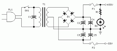
Q9_________IRF9530 100V 12A P-Channel Hexfet TransistorPower supply circuit diagram
Parts:
R1____________3K3 1/2W Resistor C1___________10nF 1000V Polyester CapacitorC2,C3______4700µF 50V Electrolytic CapacitorsC4,C5_______100nF 63V Polyester Capacitors D1__________200V 8A Diode bridgeD2__________5mm. Red LED F1,F2_______3.15A Fuses with sockets T1__________220V Primary, 25 + 25V Secondary 120VA Mains transformer PL1_________Male Mains plug SW1_________SPST Mains switchNotes:
- Can be directly connected to CD players, tuners and tape recorders. Simply add a 10K Log potentiometer (dual gang for stereo) and a switch to cope with the various sources you need.
- Q6 & Q7 must have a small U-shaped heatsink.
- Q8 & Q9 must be mounted on heatsink.
- Adjust R11 to set quiescent current at 100mA (best measured with an Avo-meter connected in series to Q8 Drain) with no input signal.
- A correct grounding is very important to eliminate hum and ground loops. Connect to the same point the ground sides of R1, R4, R9, C3 to C8. Connect C11 to output ground. Then connect separately the input and output grounds to power supply ground.
- An earlier prototype of this amplifier was recently inspected and tested again after 15 years of use.
Technical data:
Output power:
well in excess of 25 Watt RMS @ 8 Ohm (1KHz sine wave)
Sensitivity:
200mV input for 25W output
Frequency response:
30Hz to 20KHz-1dB
Total harmonic distortion @ 1KHz:
0.1W 0.014% 1W 0.006% 10W 0.006% 20W0.007% 25W 0.01%
Total harmonic distortion @10KHz:
0.1W 0.024% 1W 0.016% 10W 0.02% 20W0.045% 25W 0.07%
Unconditionally stable on capacitive loads

Friday, October 24, 2014
Modem for Digital Modes Circuits Diagram
Ham Com is a modem for almost all types of digital transmission for radio amateurs. It can be used to RTTY, ASCII, NevTex, Sitor, Amtor, Fec, CW, FSK, etc.. The modem is simple and can even be used for receiving faxes and SSTV wx-using JV-FAX software.
Modem for Digital Modes Circuits Diagram
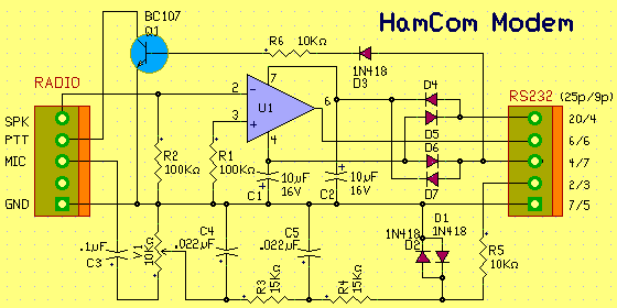
To use this modem, you need a PC with serial port, Software HamCom and radio equipment.
Modem for Digital Modes Circuits Diagram
To use this modem, you need a PC with serial port, Software HamCom and radio equipment.
25 Watt Audio Amplifier Circuits Diagram
25 Watt Audio Amplifier Circuits Diagram
Parts:
R1,R4_________47K 1/4W Resistors
R2____________4K7 1/4W ResistorR3____________1K5 1/4W ResistorR5__________390R 1/4W ResistorR6__________470R 1/4W ResistorR7___________33K 1/4W ResistorR8__________150K 1/4W ResistorR9___________15K 1/4W ResistorR10__________27R 1/4W ResistorR11_________500R 1/2W Trimmer Cermet
R12,R13,R16__10R 1/4W Resistors
R14,R15_____220R 1/4W Resistors
R17___________8R2 2W ResistorR18____________R22 4W Resistor (wirewound)
C1___________470nF 63V Polyester CapacitorC2___________330pF 63V Polystyrene CapacitorC3,C5________470µF 63V Electrolytic Capacitors
C4,C6,C8,C11_100nF 63V Polyester Capacitors
C7___________100µF 25V Electrolytic CapacitorC9____________10pF 63V Polystyrene CapacitorC10____________1µF 63V Polyester CapacitorQ1-Q5______BC560C 45V 100mA Low noise High gain PNP TransistorsQ6_________BD140 80V 1.5A PNP TransistorQ7_________BD139 80V 1.5A NPN TransistorQ8_________IRF530 100V 14A N-Channel Hexfet Transistor
Q9_________IRF9530 100V 12A P-Channel Hexfet TransistorPower supply circuit diagram
Parts:
R1____________3K3 1/2W Resistor C1___________10nF 1000V Polyester CapacitorC2,C3______4700µF 50V Electrolytic CapacitorsC4,C5_______100nF 63V Polyester Capacitors D1__________200V 8A Diode bridgeD2__________5mm. Red LED F1,F2_______3.15A Fuses with sockets T1__________220V Primary, 25 + 25V Secondary 120VA Mains transformer PL1_________Male Mains plug SW1_________SPST Mains switchNotes:
- Can be directly connected to CD players, tuners and tape recorders. Simply add a 10K Log potentiometer (dual gang for stereo) and a switch to cope with the various sources you need.
- Q6 & Q7 must have a small U-shaped heatsink.
- Q8 & Q9 must be mounted on heatsink.
- Adjust R11 to set quiescent current at 100mA (best measured with an Avo-meter connected in series to Q8 Drain) with no input signal.
- A correct grounding is very important to eliminate hum and ground loops. Connect to the same point the ground sides of R1, R4, R9, C3 to C8. Connect C11 to output ground. Then connect separately the input and output grounds to power supply ground.
- An earlier prototype of this amplifier was recently inspected and tested again after 15 years of use.
Technical data:
Output power:
well in excess of 25 Watt RMS @ 8 Ohm (1KHz sine wave)
Sensitivity:
200mV input for 25W output
Frequency response:
30Hz to 20KHz-1dB
Total harmonic distortion @ 1KHz:
0.1W 0.014% 1W 0.006% 10W 0.006% 20W0.007% 25W 0.01%
Total harmonic distortion @10KHz:
0.1W 0.024% 1W 0.016% 10W 0.02% 20W0.045% 25W 0.07%
Unconditionally stable on capacitive loads
Thursday, October 23, 2014
Build a 18W Audio Amplifier Circuits Diagram
18W Audio Amplifier Circuits Diagram

Amplifier parts:
P1_____________22K Log. Potentiometer (Dual-gang for stereo)R1______________1K 1/4W ResistorR2______________4K7 1/4W Resistor
R3____________100R 1/4W ResistorR4______________4K7 1/4W Resistor
R5_____________82K 1/4W ResistorR6_____________10R 1/2W ResistorR7_______________R22 4W Resistor (wirewound)
R8______________1K 1/2W Trimmer Cermet (optional) C1____________470nF 63V Polyester CapacitorC2,C5_________100µF 3V Tantalum bead Capacitors
C3,C4_________470µF 25V Electrolytic Capacitors
C6____________100nF 63V Polyester CapacitorD1___________1N4148 75V 150mA DiodeIC1________TLE2141C Low noise, high voltage, high slew-rate Op-ampQ1____________BC182 50V 100mA NPN TransistorQ2____________BC212 50V 100mA PNP TransistorQ3___________TIP42A 60V 6A PNP Transistor
Q4___________TIP41A 60V 6A NPN Transistor
J1______________RCA audio input socketPower supply parts:
R9______________2K2 1/4W Resistor
C7,C8________4700µF 25V Electrolytic CapacitorsD2_____________100V 4A Diode bridgeD3_____________5mm. Red LED
T1_____________220V Primary, 15 + 15V Secondary, 50VA Mains transformer PL1____________Male Mains plug
SW1____________SPST Mains switch
Notes:
- Can be directly connected to CD players, tuners and tape recorders.
- Do not exceed 23 + 23V supply.
- Q3 and Q4 must be mounted on heatsink.
- D1 must be in thermal contact with Q1.
- Quiescent current (best measured with an Avo-meter in series with Q3 Emitter) is not critical.
- Adjust R3 to read a current between 20 to 30 mA with no input signal.
- To facilitate quiescent current setting add R8 (optional).
- A correct grounding is very important to eliminate hum and ground loops. Connect to the same point the ground sides of J1, P1, C2, C3 & C4. Connect C6 to the output ground.
- Then connect separately the input and output grounds to the power supply ground.
Output power:
18 Watt RMS into 8 Ohm (1KHz sine wave)
Sensitivity:
150mV input for 18W output
Frequency response:
30Hz to 20KHz-1dB
Total harmonic distortion @ 1KHz:
0.1W 0.02% 1W 0.01% 5W 0.01% 10W0.03%
Total harmonic distortion @10KHz:
0.1W 0.04% 1W 0.05% 5W 0.06% 10W0.15%
Unconditionally stable on capacitive loads
Simple and hold circuit using op amp Circuits Diagram
As the name indicates , a sample and hold circuit is a circuit which samples an input signal and holds onto its last sampled value until the input is sampled again. Sample and hold circuits are commonly used in analogue to digital converts, communication circuits, PWM circuits etc. The circuit shown below is of a sample and hold circuit based on uA 741 opamp , n-channel E MOSFET BS170 and few passive components.
Description
As the name indicates , a sample and hold circuit is a circuit which samples an input signal and holds onto its last sampled value until the input is sampled again. Sample and hold circuits are commonly used in analogue to digital converts, communication circuits, PWM circuits etc. The circuit shown below is of a sample and hold circuit based on uA 741 opamp , n-channel E MOSFET BS170 and few passive components.
In the circuit MOSFET BS170 (Q1) works as a switch while opamp uA741 is wired as a voltage follower. The signal to be sampled (Vin) is applied to the drain of MOSFET while the sample and hold control voltage (Vs) is applied to the source of the MOSFET. The source pin of the MOSFET is connected to the non inverting input of the opamp through the resistor R3. C1 which is a polyester capacitor serves as the charge storing device. Resistor R2 serves as the load resistor while preset R1 is used for adjusting the offset voltage.
During the positive half cycle of the Vs, the MOSFET is ON which acts like a closed switch and the capacitor C1 is charged by the Vin and the same voltage (Vin) appears at the output of the opamp. When Vs is zero MOSFET is switched off and the only discharge path for C1 is through the inverting input of the opamp. Since the input impedance of the opamp is too high the voltage Vin is retained and it appears at the output of the opamp.
Circuit diagram

Sample and Hold circuit using uA741 opamp
Input and output waveforms.

Input and output waveforms - Sample and hold circuit
Notes
- The circuit can be assembled on a vero board.
- Use +15V/-15V DC dual supply for powering the opamp.
- Capacitor C1 must have minimum leakage current possible and thats why a polyester capacitor is used here.
- Mount the IC uA741 on a holder.
- The type number of the MOSFET Q1 is not very significant here and so substitution is possible if BS170 is not available.
- BS170 is a 60V, 500mA n-channel enhancement mode MOSFET available in TO-92 package.
- Preset resistor R1 can be used for offset adjustments.
Friday, September 12, 2014
6 12 Volt audio amplifier circuits
The above is an amplifier circuit using supply voltages from 6 volts DC to 12 Volt DC. Power output of the amplifier is quite low with only 1 Watt 8 ohm impedance. You can apply this to the audio signal amplifiers that require strengthening are not so large as in the pocket radio.Part List :
R1 = 100K
R2 = 39R
R3 = 100R
C1 = 100nF
C2 = 100uF
C3 = 100uF
C4 = 100uF
C5 = 470uF
C6 = 100nF
C7 = 68pF
C8 = 1nF
C9 = 47uF
IC = SFC2790C
Wednesday, August 27, 2014
Polarity protection circuits
The most simple polarity protection tehnique is to connect a series diode to the power line input. The diode conducts only when the power supply protection is correct. But the incovenient is that at higher current levels, the voltage drops and power loss of the diode affects the power level adversely.
![polarity]() This polarity protection circuit is dimensioned for 12 V power supplies and avoids the voltage and power loss problem. By correct polarity, the current flowing to the D1 and the relay coil causes the relay contacts to activate. The NO contact closes powering the electronic device. The NC contact opens and the current supplying the relay coil is reduced to a low level just enough to maintain relay activation.
This polarity protection circuit is dimensioned for 12 V power supplies and avoids the voltage and power loss problem. By correct polarity, the current flowing to the D1 and the relay coil causes the relay contacts to activate. The NO contact closes powering the electronic device. The NC contact opens and the current supplying the relay coil is reduced to a low level just enough to maintain relay activation.
source [link]
Read More..
source [link]
Subscribe to:
Posts (Atom)
