Showing posts with label build. Show all posts
Showing posts with label build. Show all posts
Saturday, October 25, 2014
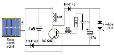
Build a Solar Garden Light Circuit Diagram
This is a Solar Garden Light Circuit Diagram that consists of a very simple system garden lighting that can be done by using some common electronic parts and a small solar panel. The electronic design is simple yet very efficient, has the advantage of being solar powered, it requires only one transistor, one 2.5 volt solar panel and some other common electronic components you can remove junk.
This solar lighting system automatically turns on the LEDs when the solar panel detects no light turns off when the solar panel produces more than 1v and charges the battery when the panel produces more than 2.1V
The coils in this circuit require a core material F29 and they must be made with wire of 0.095 mm in core 2.6x6mm. "This circuit uses the system joule thief (joule thief) to provide voltage necessary for the LED, so other coils can be tested.
The coils in this circuit require a core material F29 and they must be made with wire of 0.095 mm in core 2.6x6mm. "This circuit uses the system joule thief (joule thief) to provide voltage necessary for the LED, so other coils can be tested.
Solar Garden Light Circuit Diagram

Friday, October 24, 2014
Build a Wire Break Alarm With Delay Circuit Diagram
Here is a simple circuit of wire-break alarm that activates after a delay of 15 to 30 seconds. When the thin-wire loop running across the entrance door is broken, the alarm sounds after a delay of 15 to 30 seconds, the time period set through VR1. Thus the occupants get sufficient time to lock the room from the outside and catch the thief.
The circuit uses CD4060, which is a 14-stage ripple-carry binary counter/divider and oscillator. It is wired as a timer here and does not need input pulse for trigger. CD4060 gets activated as soon as the power supply is switched on. Output O13 of CD4060 goes high after the lapse of preset delay set through VR1. Transistor SL100 (T2) is wired as a switch to power the timer section built around CD4060. When the wire loop is closed, transistor T2 does not conduct. So power to the timer circuit is not available and the piezobuzzer does not sound.
Wire-Break Alarm With Delay Circuit Schematic

On the other hand, when the wire loop is broken by some intruder, transistor T2 conducts to power the circuit and the piezobuzzer sounds after 15 to 30 seconds. IC1 can be reset by connecting the wire loop or interrupting the supply. The circuit works off regulated 9V-12V. Assemble it on a general-purpose PCB and enclose in a metallic or plastic box of appropriate size. Connect piezobuzzer PZ1 through external wires and complete the installation.
Thursday, October 23, 2014
Build a 18W Audio Amplifier Circuits Diagram
18W Audio Amplifier Circuits Diagram

Amplifier parts:
P1_____________22K Log. Potentiometer (Dual-gang for stereo)R1______________1K 1/4W ResistorR2______________4K7 1/4W Resistor
R3____________100R 1/4W ResistorR4______________4K7 1/4W Resistor
R5_____________82K 1/4W ResistorR6_____________10R 1/2W ResistorR7_______________R22 4W Resistor (wirewound)
R8______________1K 1/2W Trimmer Cermet (optional) C1____________470nF 63V Polyester CapacitorC2,C5_________100µF 3V Tantalum bead Capacitors
C3,C4_________470µF 25V Electrolytic Capacitors
C6____________100nF 63V Polyester CapacitorD1___________1N4148 75V 150mA DiodeIC1________TLE2141C Low noise, high voltage, high slew-rate Op-ampQ1____________BC182 50V 100mA NPN TransistorQ2____________BC212 50V 100mA PNP TransistorQ3___________TIP42A 60V 6A PNP Transistor
Q4___________TIP41A 60V 6A NPN Transistor
J1______________RCA audio input socketPower supply parts:
R9______________2K2 1/4W Resistor
C7,C8________4700µF 25V Electrolytic CapacitorsD2_____________100V 4A Diode bridgeD3_____________5mm. Red LED
T1_____________220V Primary, 15 + 15V Secondary, 50VA Mains transformer PL1____________Male Mains plug
SW1____________SPST Mains switch
Notes:
- Can be directly connected to CD players, tuners and tape recorders.
- Do not exceed 23 + 23V supply.
- Q3 and Q4 must be mounted on heatsink.
- D1 must be in thermal contact with Q1.
- Quiescent current (best measured with an Avo-meter in series with Q3 Emitter) is not critical.
- Adjust R3 to read a current between 20 to 30 mA with no input signal.
- To facilitate quiescent current setting add R8 (optional).
- A correct grounding is very important to eliminate hum and ground loops. Connect to the same point the ground sides of J1, P1, C2, C3 & C4. Connect C6 to the output ground.
- Then connect separately the input and output grounds to the power supply ground.
Output power:
18 Watt RMS into 8 Ohm (1KHz sine wave)
Sensitivity:
150mV input for 18W output
Frequency response:
30Hz to 20KHz-1dB
Total harmonic distortion @ 1KHz:
0.1W 0.02% 1W 0.01% 5W 0.01% 10W0.03%
Total harmonic distortion @10KHz:
0.1W 0.04% 1W 0.05% 5W 0.06% 10W0.15%
Unconditionally stable on capacitive loads
Wednesday, October 15, 2014
Build a Digital Theremin Circuit Diagram
Theremin circuit shown in this schematic diagram uses digital component, so we can call it a digital Theremin. This circuit employs logic inverter 74C04 or CD4069 hex inverter and CD4046 phase-locked-loop (PLL) IC.
The CD4069 logic inverter is operated as a fixed-frequency oscillator with frequency around 100kHz. The CD4046 is operated as a variable frequency oscillator which is adjustable around 100kHz. The exact center frequency of the on-chip oscillator is determined by R4, C2 and R3. Here is the schematic diagram of the circuit.
Digital Theremin Circuit Diagram

The frequency of variable oscillator frequency circuit can be shifted several kilohertz by moving your hand approaching the antenna since the C2 and the antenna form an equivalent parallel capacitance. The frequency of the variable oscillator should be set to the same frequency of fixed oscillator when there is no hand or human body close to the antenna.
This calibration is done by adjusting the zero control R4 pot with this simple rule: If both oscillators (the fixed and the variable) are set to the same frequency then the Theremin will produce no output (silent). This Theremin circuit will start producing audible tone if you move your hand approaching the antenna since it will shift the frequency of the variable oscillator. You can play this Theremin circuit by moving your right hand around the antenna and at the same time turning the volume knob R5 with your left hand.
Build a Theremin with Inverter Gates
This simple but complete Theremin with Inverter Gates is constructed using only two inverter chip plus one regulator IC. This Theremin circuit consist of five functional blocks: power supply regulator, hand controlled oscillator, null oscillator, mixer, and filter. Here is the complete schematic diagram.
Theremin with Inverter Gates schematic diagram

Voltage Regulator and Circuit Protector
The power supply regulator consist of LP2950 regulator IC, which stabilize the voltage from battery to 5V. You can use more popular 7805 IC for this, but since the power consumption of this Theremin circuit is very small, then you can use 78L05 which is smaller. CR1 diode is used to protect from inappropriate battery polarity, shorting the battery voltage together with R8 100 Ohm resistor which prevent the large current when the battery is installed in wrong direction. Although the inverter chip will work well for 9V battery, there is a benefit of using voltage regulation to regulate the battery voltage at lower voltage level, that the voltage will remain constant for until the end of battery life. This will avoid frequency drift of the Theremin’s null oscillator which should be carefully adjusted to zero the output frequency, which can be affected by the supply voltage.
Hand Controlled Oscillator
The hand proximity sensor is an oscillator which has antenna extension which shift the capacity coupling in the loop. This capacitance shift occur when we move our hand approaching the antenna. Since this change is very small in percentage, we need this oscillator to be high enough to produce notable frequency difference. This oscillator block is built around U1A, U1B, and U1C. This oscillator give oscillation at around 73kHz. This frequency is not directly audible, we have to process this signal further to produce audible signal.
Null Oscillator
Null oscillator is employed to produce a constant frequency oscillation that will be used to produce differential frequency which is audible. This oscillator block is built around U2A, U2B, and U2C. This null oscillator should be adjustable to set the null point where the Theremin should produce no oscillation at certain hand position. At this point, the null oscillator should be adjusted to have same frequency with the hand controlled oscillator since the audible Theremin output is the product of the difference between hand controlled and null oscillator frequencies.
Frequency Mixer (Differentiator)
The mixer is used to mix the signal from two oscillators, the hand controlled and the null oscillators. This mixer produce an output which contain many frequency components, not only the difference but also the original and the sum, since the amplifier U1F is basically a digital inverter which has non-linear transfer function. Fortunately, all the frequency components, except the difference, will be much higher than the needed signal and inaudible. This make it easy to remove by simple low pass filter to obtain only the differential frequency component.
Low Pass Filter
As stated before, we need to obtain only the audible frequency component by low-pass filtering. Although the high frequencies is inaudible, we still have to remove it since it can cause damage in audio power amplifier is the level is too high. It can distort the audible signal, and it can eat the electric power like ghost, frying your amplifier or at least make it overheated. This Theremin circuit use simple low pass filter consist of C4, R5, and R7 for the passive stage, and C2 inside the inverter amp loop.
Saturday, September 20, 2014
Build a 500W low cost 12V to 220V Inverter Circuit Diagram
Build a 500W low cost 12V to 220V Inverter Circuit Diagram. Using this circuit you can convert the 12V dc in to the 220V Ac. In this circuit 4047 is use to generate the square wave of 50hz and amplify the current and then amplify the voltage by using the step transformer.
500W low cost 12V to 220V Inverter Circuit Diagram
How to calculate transformer rating
The basic formula is P=VI and between input output of the transformer we have Power input = Power output
For example if we want a 220W output at 220V then we need 1A at the output. Then at the input we must have at least 18.3V at 12V because: 12V*18.3 = 220v*1
So you have to wind the step up transformer 12v to 220v but input winding must be capable to bear 20A.
Attention: This Circuit is using high voltage that is lethal. Please take appropriate precautions
Author:Ashad Mustufa, mustufa66@hotmail.com
Sunday, September 14, 2014
Build a Zero Crossing Switch Wiring diagram Schematic
This is a simple Zero Crossing Switch Circuit Diagram. The zero-crossing is important for systems which send digital data over AC diagram, such as modems, X10 home automation control systems, and Digital Command Control type systems for Lionel and other AC model trains. When switching loads with the aid of a thyristor, a large amount of RFI can be generated unless some form of zero crossing switch is used.
Zero Crossing Switch Circuit Diagram

The schema shows a simple single transistor zero crossing switch. Rl and R2 act as a potential divider. The potential at their junction is about 10% of the ac voltage. This voltage level is fed, via R3, to the transistor`s base. If the voltage at this point is above 0, the transistor will conduct, shunting any thyristor gate current to ground. When the line potential is less than about 2 V, it is possible to trigger the thyristor.
The diode Dl is to remove any negative potential that might cause reverse breakdown. If electrical power is to be switched, no electrical interference is generated if switched at an instant when there is no current a zero crossing. Early light dimmers and similar devices generated interference; later versions were designed to switch at the zero crossing.
Thursday, September 11, 2014
Build a Portable Nicad Battery Charger Wiring diagram Schematic
This is a Portable Nicad Battery Charger Circuit Diagram. This schema can you build easily, The portable charger is intended primarily to give model enthusiasts the opportunity of charging their Nicad batteries from a car battery out in the open. The supply voltage for the schema is regulated by IC1. When the schema is connected to the car battery, D2 lights only if the Nicad to be charged has been connected with correct polarity. For that purpose, the + terminal of the Nicad battery is connected to the base of T1 via R8. Because even a discharged battery provides some voltage, T1 is switched on and D2 lights.
Portable Nicad Battery Charger Circuit Diagram
Only if the polarity is correct will the pressing of the start switch, SI, have any effect. If so, the collector voltage of T1 is virtually zero so that monostable IC2 is triggered by SI. The output, pin 3, of this CMOS timer then becomes high, T2 is switched on and relay Rel is energized. Charging of the Nicad battery, via R5 and D6, then begins and charging indicator D4 lights. During the charging, C4 is charged slowly via PI and R4. The value of these components determines the mono time of IC2 and thus the charging period of the Nicad battery. With values as shown in the diagram, that period can be set with PI to between 26 and 33 min. Notice that this time is affected by the leakage current of C4; use a good-quality capacitor here.
The charging can be interrupted with reset switch S2. The charging current through the Nicad battery is determined by the value of R, which can be calculated: Ic is the charging current, which is here because the chosen charging period is twice the nominal value of the capacity of the Nicad battery. Resistor R must be able to dissipate a power of 1/ R W. Finally, make sure that the Nicad battery is suitable for fast charging; never charge for longer than half an hour!
Build a Simple 10 Watt Power Amplifier Wiring diagram Schematic
The aim of the project was to make an audio amplifier that can deliver up to 10W R.M.S. power output.
Risk of instability if no input connected. When testing, connect R (about 3k3).
Needs well smoothed power supply of about 20 to 30 volts. Peak power is well over 10 Watts.
The table below shows the approximate voltages to be expected when using a 24v supply and with the variable resistor set to give a current of about 40mA in the output stage.
| ||||||||||||||||||
Transistors:
Tr1 BCY70 (or BC 182L or BC212L or BC214L)
Tr2/3/4 BFY50/51
Tr5 BFX88
Tr6/7 2N3055
Tr1 BCY70 (or BC 182L or BC212L or BC214L)
Tr2/3/4 BFY50/51
Tr5 BFX88
Tr6/7 2N3055
Simple 10 Watt Power Amplifier Circuit Diagram
Component Side
Copper Side
Saturday, September 6, 2014
Build a Power Doorbell Wiring diagram Schematic
Build a Power Doorbell Circuit Diagram, In this schema define when the doorbell switch is pressed, the two monostable stages are activated in sequence, applying bias to a pair of voltage-controlled resistor stages. These then modulate the outputs from a pair of tone generators. The resulting signals are fed to an audio amplifier, then to the speaker.Read: Simple Electronic Music Maker Circuit Diagram
Power Doorbell Circuit Diagram

Wednesday, September 3, 2014
Build a Fast half wave Rectifier Wiring diagram Schematic
Precision half wave rectifier using an operational amplifier will have a rectification accuracy of 1% from dc to 100 kHz.
Fast half-wave Rectifier Circuit Diagram

If you like this dont forget click on share button
Fast half-wave Rectifier Circuit Diagram
If you like this dont forget click on share button
Build a high volt supply Wiring diagram Schematic
A light dimmer, a 1 µf capacitor and a 12 V car ignition coil form the simple line powered HV generator. The current in the dimmer is shown in Fig. B. At times tp t2, set by the dimmer switch, the inner triac of the dimmer switches on, and a very high and very fast current pulse charges the capacitor through the primary of the induction coil.
Then at a rate of 120 times per second for a 60 Hz line, a very high voltage pulse appears at the secondary of the coil. To obtain an HV dc output, use a voltage doubler. Dl and D2 are selenium rectifiers (TV 18 Siemens or ITT) used for the supply of television sets. High value output shock protection resistors, R, are recommended when suitable.
Build a high-volt supply Circuit Diagram
Tuesday, September 2, 2014
Build a Passive Infrared Sensor Wiring diagram Schematic
What is PIR ?Passive Infrared Sensor Circuit Diagram. Detectors or pyroelectric sensors, passive infrared or PIR sensor, are made of a crystalline material that generates an electric charge on the surface when exposed to heat in the form of infrared radiation. When radiation increases the amount of electrical charge increases too and this load is measured with a sensitive FET transistor which is inside the sensor module.

With the RIP is commonly used as a motion detector of an object by detecting the infrared signal radiated from the object (people and animals). The Passive Infrared Sensors are also used in remote thermometers.
Pinning PIR sensor
Pin 1 of the PIR must be connected to the positive supply 5V DC. Pin 2 is the output of PIR sensor, it must have a connection to the earth through a resistor of 47K to 100K (depending on the schema). Pin 3 of the RIP must be connected to ground or negative schema.
Simple Circuit Diagram using PIR Sensor
Simple schema motion sensor PIR detector.
Connect the PIR sensor in Arduino
The image above shows a PIR sensor as a switch connected to an Arduino board using a 10k pull-down resistor.
Monday, September 1, 2014
Build a 3 Channels LED Flasher Wiring diagram Schematic
Build a 3 Channels LED Flasher Circuit Diagram. Inserting two 1-MO resistors, R1 and R2, in the output stage of one of the schema`s inverters limits the current needed by the oscillator tone more than a few pA. This schema includes a CD4007 package, which has three CMOS inverters. It forms a standard three-inverter oscillator. Resistors R1 and R2, in series with separate drains on inverter pins 8 and 13, limit the oscillator`s supply current. Capacitor C1 and resistors R5 set the off time of the oscillator, C1; R6 sets the on time.
Three Years LED Flasher Circuit Diagram
A VN10KM small-power FET, current limited by R4, drives two HLMP-3300 LEDs. The LEDs consume about 20 mA for 1 ms. Their average current determines battery life. Since the LEDs in the schema flash at 1 Hz, the average current drain is about 1/1000 of 20 mA, or 20 p.A. A 9-V battery should last about three years at the current drain-essentially the shelf life of an alkaline battery.
Sunday, August 31, 2014
Build a Voltage To Frequency Converter Wiring diagram Schematic 2
Build a Voltage-To-Frequency Converter Circuit Diagram 2. Using a Burr-Brown VFC 32 IC, this voltage-to-frequency converter uses few components. The schema values are shown in the figure. This charge-balanced V/F converter uses a VFC32 or a VFC320 IC.
The positive charge from the 1-mA balances the negative charge from the input. V/F converter waveforms are shown in Fig. 100-l(b).
Voltage-To-Frequency Converter Circuit Diagram 2
Thursday, August 28, 2014
How to Build 1 2 30V 1 5A Variable Regulated Power supply Circuit
How to Build 1.2-30V/1.5A Variable Regulated Power supply, This is simple 1.2-30V/1.5A variable regulated power supply schema diagram The 110V-AC coming from the powercord is fed to the transformer TR1 via the on-off switch and the 500mA fuse. The 30vac output (approximately) from the transformer is presented to the BR1, the bridge-rectifier, and here rectified from AC (Alternating Current) to DC (Direct Current). If you dont want to spend the money for a Bridge Rectifier, you can easily use four general purpose 1N4004 diodes. The pulsating DC output is filtered via the 2200µF capacitor (to make it more manageable for the regulator) and fed to IN-put of the adjustable LM317 regulator (IC1). The output of this regulator is your adjustable voltage of 1.2 to 30volts varied via the Adj pin and the 5K potmeter P1. The large value of C1 makes for a good, low ripple output voltage.
1.2-30V/1.5A Variable Regulated Power supply Circuit Diagram
Why exactly 1.2V and not 0-volt? Very basic, the job of the regulator is two-fold; first, it compares the output voltage to an internal reference and controls the output voltage so that it remains constant, and second, it provides a method for adjusting the output voltage to the level you want by using a potentriometer. Internally the regulator uses a zener diode to provide a fixed reference voltage of 1.2 volt across the external resistor R2. (This resistor is usually around 240 ohms, but 220 ohms will work fine without any problems). Because of this the voltage at the output can never decrease below 1.2 volts, but as the potentiometer (P1) increases in resistance the voltage accross it, due to current from the regulator plus current from R2, its voltage increases. This increases the output voltage.
D1 is a general purpose 1N4001 diode, used as a feedback blocker. It steers any current that might be coming from the device under power around the regulator to prevent the regulator from being damaged. Such reverse currents usually occur when devices are powered down.
The ON Led will be lit via the 18K resistor R1. The current through the led will be between 12 - 20mA @ 2V depending on the type and color Led you are using. C2 is a 0.1µF (100nF) decoupler capacitor to filter out the transient noise which can be induced into the supply by stray magnetic fields. Under normal conditions this capacitor is only required if the regulator is far away from the filter cap, but I added it anyway. C3 improves transient response. This means that while the regulator may perform perfectly at DC and at low frequencies, (regulating the voltage regardless of the load current), at higher frequencies it may be less effective. Adding this 1 µF capacitor should improve the response at those frequencies.
R3 and the trimmer pot (P2) alows you to zero your meter to a set voltage. The meter is a 30Volt type with an internal resistance of 85 ohms. I you have or obtained a meter with a different Ri (internal resistance) you will have to adjust R3 to keep the current of meter to 1mA. Just another note in regards this meter, use the reading as a guideline. The reading may or may not be off by about 0.75volts at full scale, meaning if your meter indicates 30 volts it may be in reality almost 31 volts or 29 volts. If you need a more precies voltage, then use your multimeter.
Construction:
Because of the few components you can use a small case but use whatever you have available. I used a power cord from a computer and cut the computer end off. All computer power cords are three-prong. The ground wire, which is connected to the middle pin of the power plug is connected to the chassis. The color of the ground-wire is either green or green/yellow. It is there for your protection if the 110vac accidentally comes in contact with the supply housing (case). BE CAREFUL always to disconnect the powerplug when you working inside the chassis. If you choose to use an in-line, or clip-type fuseholder be sure to isolate it with heat shrink or something to minimize accidental touching.
I use perf-board (or Vero board) as a schema board. This stuff is widely available and comes relatively cheap. It is either made of some sort of fiber material or Phenolic or Bakelite pcb. They all work great. Some Phenolic boards come with copper tracks already on them which will make soldering the project together easier.
I mounted the LM317(T) regulator on a heatsink. If you use a metal/aluminum case you can mount it right to the metal case, insulated with the mica insulator and the nylon washer around the mounting screw. Note that the metal tab of the LM317 is connected internally to the Output pin. So it has to be insulated when mounting directly to the case. Use heat sink compound (comes in transparent or white color) on the metal tab and mica insulator to maximize proper heat transfer between LM317 and case/ or heatsink.
Drill the holes for the banana jacks, on/off switch, and LED and make the cut-out for the meter. It is best to mount everything in such a way that you are able to trouble-shoot your schema board with ease if needed. One more note about the on-off switch S1, this switch has 110VAC power to it. After soldering, insulate the bare spots with a bit of silicon gel. Works great and prevents electrical shock through accidental touching.
If all is well, and you are finished assembling and soldering everything, check all connections. Check capacitors C1 & C3 for proper polarity (especially for C1, polarity reversal may cause explosion). Hookup a multimeter to the power supply output jacks. Set the meter for DC volts. Switch on S1 (led will light, no smoke or sparks?) and watch the meter movement. Adjust the potentiometer until it reads on your multimeter 15Volts. Adjust trimpot P2 until the meter also reads 15volts. When done, note any discrepancies between your multimeter and the power supply meter at full scale (max output). Maybe there is none, maybe there is a little, but you will be aware of it. Good luck and have fun building!

Parts List
BR1 = Bridge Rectifier, 100V - 3A C1 = 2200 µF, 63V
IC1 = LM317, adjustable regulator C2 = 0.1 µF
V = Meter, 30V, Ri = 85 ohm C3 = 1µF, 40V
TR1 = Transformer, 25V, 2A Plug = 3-wire plug & cord
R1 = 18K, 5% S1 = On-Off toggle switch
R2 = 220 ohm, 5% D1 = 1N4001
R3 = 27K, 5% Fuse = 110V, 500mA, slow-blow
P1 = 5K, potentiometer FuseHolder, wire, solder, case, knob for P1
P2 = 10K, 10-turn trim-pot Red & Black Banana Jacks
Notes:
This is a simple, but low-ripple powersupply, and an excellent project if youre starting out in electronics. It will suit your needs for most of your bench testing and prototype applications. The output is adjustable from 1.2 volts to about 30 volts. Maximum current is about 1.5 amps which is also sufficient for most of your tinkering. It is relatively easy to build and can be pretty cheap if you have some or all the required parts. A printed schema board is not included and Im not planning on adding one since the whole thing can easily be build on perferated or vero board. Or buy one of Radio Shack/Tandys experimentors boards (#276-150). Suit yourself. The meter and the transformer are the money suckers, but if you can scrounge them up from somewhere it will reduce the cost significantly. BR1 is a full-wave bridge rectifier. The two ~ denotes AC and are connected to the 25vac output coming from the transformer. IC1 is a 3-pin, TO-220 model. Be sure to put a cooling rib on IC1, at its max 1.5 A current it quickly becomes very hot..
All the parts can be obtained from your local Radio Shack or Tandy store. The physical size of the power supply case depends largely on the size of the meter & transformer. But almost anything will do. Go wild.
Sourced By Tony van roon
Subscribe to:
Posts (Atom)
