Showing posts with label voltage. Show all posts

Tuesday, October 28, 2014

70 260VAC to180 350VDC voltage converter


Using circuit diagram below can be built a voltage converter, able to convert a 70-260V AC to a 180-350V DC voltage.

For this, a rectifier contained in a MC34161 is used, as a voltage doubler for low input voltages and as rectifier for high standard input voltage.

A variation of four times of the input voltage is reflected in a variation of not more than two times in output voltage.

MC34161 has included a reference voltage source which supplies a voltage of 2.54 V to pin 1. The signal applied to pin 2 is compared with internal voltage of 1.27 V.

R2-R3 voltage divider provides change state of internal comparator which grow output input voltage over 135 V (pin 5 passes in 1 state). The potential at pin 2 is less than 1.27 V. Triac is blocked and disconnects median connection between the two output capacitors, C2 and C3, such that doubling output voltage can not be produced

70-260VAC

  • When the input voltage is less than 135 V, pin 2 is maintained above the potential value of 1.27 V
  • Diodes D2 and D3 and capacitors C2 and C3 will function as voltage doubler.
  • Zener diode D5, together with R1 and C4, integrated circuit provides power to a stable source of 12 V. The time required passing standard rectifier circuit of the voltage doubler is determined by R4-C1.
  • Operating voltage of capacitors C2 and C3 must be> 250 V.

Read More..

Friday, October 24, 2014

12KV High Voltage Generator

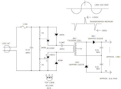
The hobby circuit below uses an unusual method to generate about 12,000 volts with about 5uA of current. Two SCRs form two pulse generator circuits. The two SCRs discharge a 0.047uF a 400v capacitor through a xenon lamp trigger coil at 120 times a second.
Circuit Project:12KV High Voltage Generator
The high voltage pulses produced at the secondary of the trigger coil are rectified using two 6KV damper diodes. The voltage doubler circuit at the secondary of the trigger coil charges up two high voltage disc capacitors up to about 12KV. Although this circuit can’t produce a lot of current be very careful with it. A 12KV spark can jump about 0.75 of an inch so the electronic circuit needs to be carefully wired with lots of space between components.
Source: DiscoverCircuits
Read More..

Monday, October 20, 2014

Adjustable Voltage and Variable Current Limiter Circuit Diagram

This Mini Voltage Source with Adjustable Current Limit variable is very simple and efficient, ideal for small shippers or circuits that require a current limiter with adjustable voltage that this circuit can vary from a few mA up to 2 A and voltage 1.225v up to 12V or more, depending on the power supply. 

Once the current reaches the limit set by the 100R resistor, transistor BC547 begins to act on the voltage regulator in the Adj pin and the output voltage starts to decrease. If the output is shorted, the output voltage will reduce to almost zero, as a kind of protection.

Adjustable Voltage and Variable Current Limiter Circuit Diagram

Adjustable Voltage and Variable Current Limiter Circuit Diagram


Adjustable Voltage and Variable Current Limiter Circuit Diagram
Read More..

Sunday, October 19, 2014

2 36V 10A High Current Variable Voltage Regulator

Yesterday I no enhance the circuit in my blog. Today lead High Current power supply 10A and Can Adjustable Voltage or Variable Voltage Regulator 2V to 36V. By the prominent point of this circuit. Be there is the a little equipment and is simple have VR1 for control Volt output. For the equipment must use the size is appropriate. If use the a little value goes to get Current not tall on schedule keep, such as The Transformer use 10A, Transistor sizes should are the number that notes , and A capacitors should choose many values especially C1 – 18000 uF , use 10000uF values wasp parallel can. For other detail , friends sees in the circuit please yes.

Read More..

Saturday, October 18, 2014

5V to 12V DC LM2577 Converter step up Voltage Regulator

This is Circuit DC to DC Converter Step up Voltage Regulator From 5V To 12V 1A Regulated Output.

LM2577 (3A)
DC to DC step up voltage regulator.

Wide input voltage 3.5Vdc to 40Vdc.
Component list
- 2.2k 1/4W resistor
- 0.1uF capacitor
- 0.33uF capacitor
- 680uF 50V electrolytic capacitor
- 1N5822 high speed schottky diode (3A)
- wire coil inductor, 100uH
- “for LM2577-adj IC” 20k multi-turn variable resistor, set to ratio to R2=2k, R1=18k for voltage output of 12Vdc before soldering
Part number:
- LM2577-12 (12Vdc output)
- LM2577-15 (15Vdc output)
- LM2577-ADJ (1.23Vdc to 37Vdc output)
Read More..

Tuesday, September 23, 2014

Adjustable voltage output control by 2SC458

This again the one circuit that use in fining value output voltage, for apply give straight with the requirement of load be the circuit that is simple and have no result temperature way of the joint junction of transistor. Vout control 0V-30V at 0.1A
The principle works be transistor Q1 2SC458 that built model common-emitter amplifier, which perform fine decrease input voltage get down then heal volt that give may but at collector voltage compare with ground. Which get from the combination of voltage at base – emitter pin (0.6V) with VZener diode (6.2V) already fine the value of a resister can fine the value VR1 help transistor part Q2 2SC458 perform be compared as power supply current source and current that fixed. By current at flow come in the way base pin of Q2 and when Q2 bias current. That already Voltage output get, with fining that a resister VR1 during 5.8V-15.8V. By have R3 and C1 perform be RC Filter caution. This circuit power current source get 100mA topmost should apply to load that use current low.

s:www.eleccircuit.com
Read More..

Monday, September 22, 2014

With Time Delay High And Low Voltage Cut Off

Overview

The power line fluctuations and cut-offs cause damages to electrical appliances connected to the line. It is more serious in the case of domestic appliances like fridge and air conditioners. If a fridge is operated on low voltage, excessive current flows through the motor, which heats up, and get damaged.

The under/over voltage protection circuit with time delay presented here is a low cost and reliable circuit for protecting such equipments from damages. Whenever the power line is switched on it gets connected to the appliance only after a delay of a fixed time. If there is hi/low fluctuations beyond sets limits the appliance get disconnected. The system tries to connect the power back after the specific time delay, the delay being counted from the time of disconnection. If the power down time (time for which the voltage is beyond limits) is less than the delay time, the power resumes after the delay: If it is equal or more, then the power resumes directly.

This circuit has been designed, built and evaluated by me to use as a protector for my home refrigerator. This is designed around readily available semi-conductor devices such as standard bipolar medium power NPN transistor (D313/SL100/C1061), an 8-pin type 741 op-amp and NE555 timer IC. Its salient feature is that no relay hunting is employed. This draw back is commonly found in the proctors available in the market.

The complete circuit is consisting of various stages. They are: - Dual rail power supply, Reference voltage source, Voltage comparators for hi/low cut offs, Time delay stage and Relay driver stage. Lets now look at the step-by-step design details.

Dual rail power supply.

This is a conventional type of power supply as shown in Figure 1. The power is applied through the step-down transformer (230/12-0-12V/500mA). The DC proportional to the charging input voltage is obtained from bridge rectifier. Two electrolytics are there to bypass any spikes present. Bridge is capable of handling currents up to 1 Amp.

Output is given by: -

V(out) = 0.71 X V (secondary)

= 0.71 X 24V

= 17.04 V

(This equation is similar for the negative rail as well)

Circuit diagram

Low voltage cut off op-amp

Figure 2 shows the use of very common and easily available op-amp 741 as a comparator. The op-amp is available in TO-5 and DIP type packing.

Circuit diagram

In this ckt the zener diode D1 and it’s associated resistor R1 are connected to the non-inverting terminal (+ve) of 741 to give the suitable reference voltage. The DC voltage from the sensor is given to the inverting (-ve) terminal through pre-set R2.This is used to set the input level.

When the sensor input is less than Zener voltage the output from the Op-amp remains high and when it is greater than Zener voltage the output goes low. When the sensing voltage is equal to Zener voltage the output of the op-amp is approximately zero.

This phenomenon is used as a decision for switching the relay and to give cutoff in a low voltage situation.

High voltage cut off op-amp

Here the op-amp is used as a inverted amplifier. See Figure 3.Zener and resistor network gives reference voltage to the inverting terminal (-ve) of op-amp. Sensing voltage derived through the 10 K pre-set is given to the non- inverting (+ve) terminal and this sets the high level cut.

When the input DC from the sensor is less than Zener voltage the output of the op-amp is low and vice-versa. When the input DC voltage is equal to the zener voltage, the op-amps output is approximately zero.

Circuit diagram

Time delay

I’ve selected the 555 timer due to following reasons.

1. Timing from microseconds through hours.

2. Ability to operate from wide range of supply voltages.

3. High temperature stability.

4. Easily Available.

5. Its triggering circuit is quite sensitive.

This is basically a monostable. The external timing capacitor C2 is held initially discharged by the timer. The circuit triggers upon receiving a pulse to its pin 2 when the level reaches 1/3 Vcc. Once triggered., the circuit will remain in that state until the set time is elapsed or power to the circuit cuts off. The delayed period in seconds is 1.1 C2.R1 where R1 is in megohms and C2 is in microfarads. In practice, R1 should not exceed 20 M. If you use an electrolytic capacitor for C2, select a unit for low leakage. The time delay may have to be adjusted by varying R1 to compensate for the wide tolerance of electrolytics.


Circuit diagram

Relay Driver

The output from the voltage level detectors cannot directly drive the relay and hence the relay driver is used.

Circuit diagram

In this a relay (12V <500>

The Complete Circuit

Circuit diagram

Under normal operating conditions i.e. when the input voltage is between maximum and minimum limit the output from the both the comparators are low. The transistor Q1 is OFF and the relay is in de-energized (pole connected to N/C pin) state and the output is obtained.

When the input voltage is below or above the limits set by the pre-sets R8 or R9, the output of the Op-Amps goes either low or high and diodes D1 or D2 would be forward biased depending on the situation. Transistor Q1 switches ON and the flow of current from collector to emitter energizes the relay and the output is cutoff.

A small amount of hystersis has been added via feed back resistors R10 & R11 so that the relay turns on when the level falls to a particular value but does not turn again until it raises a substantial amount above this value. Other wise the relay contacts will frequently turn on/off and produce chattering.

Construction Hints

1) I used a piece of varoboard, which has copper strips on one side to mount the components, and housed the entire circuit and the transformer in a discarded ATX PC power supply box.

2) An autotransformer has been used to set the limits. Set the output of the autotransformer to 250V AC and connect it to the primary of transformer T1 (see Figure 1). Then adjust the pre-set R9 such that relay just energizes. This is the high limit. Next set the output of the autotransformer to 200V AC and adjust the pre-set R8 such that the relay energizes. Please note that these are my preferred limits but you may select any range from say 170 to 270V AC.

3) A neon with a suitable resistor could be connected between the AC supply lines as an ON indicator. Alternatively, LED with a current limiting resistor could be connected between the relay coil so when the relay is energized LED will indicate the situation. 

Read More..

Friday, September 19, 2014

3v Low Battery Voltage Flasher

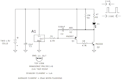
Many battery powered devices use two AA alkaline cells.  Often you will not know when it is time to replace the batteries until the device powered by them actually stops operating.  The hobby circuit below can be connected to a 3v battery, to give you some warning when the battery is nearing its end of life.

Circuit Project:3v Low Battery Voltage Flasher Circuit
 
It will flash a LED when the battery voltage drops to about 2.4 volts. The electronic circuit draws only 1ua of current in standby mode and jumps to only 20ua when flashing, so it can safely be included without depleting the battery energy. A voltage detector IC from Panasonic (Microchip also makes similar devices) is used to monitor the battery voltage. The device’s open drain output swings low, when the battery voltage is below 2.4 to 2.5 volts. This action turns on the two transistor oscillator circuit, which drives the LED with short current pulses lasting only 2ms.
Source: DiscoverCircuits
Read More..

Thursday, September 18, 2014

Low Cost Step Down Converter With Wide Input Voltage Range

The circuit described here is mostly aimed at development engineers who are looking for an economical step-down converter which offers a wide input voltage range. As a rule this type of circuit employs a step-down converter with integrated switching element. However, by using a more discrete solution it is possible to reduce the total cost of the step-down converter, especially when manufacturing in quantity. The TL5001A is a low-cost PWM controller which is ideal for this project. The input voltage range for the step-down converter described here is from 8 V to 30 V, with an output voltage of 5 V and a maximum output current of 1.5 A.


When the input voltage is applied the PWM output of IC1 is enabled, taking one end of the voltage divider formed by R1 and R2 to ground potential. The current through the voltage divider will then be at most 25 mA: this value is obtained by dividing the maximum input voltage (30 V) minus the saturation voltage of the output driver (2 V) by the total resistance of the voltage divider (1.1 kΩ). T1 and T3 together form an NPN/PNP driver stage to charge the gate capacitance of P-channel MOSFET T2 as quickly as possible, and then, at the turn-off point, discharge it again.

The base-emitter junction of T3 goes into a conducting state when the PWM output is active and a voltage is dropped across R2. T3 will then also conduct from collector to emitter and the gate capacitance of T2 will be discharged down to about 800 mV. The P-channel MOSFET will then conduct from drain to source. If the open-collector output of the controller is deactivated, a negligibly small current flows through resistor R2 and the base of T1 will be raised to the input voltage level. The base-emitter junction of T1 will then conduct and the gate capacitance of T2 will be charged up to the input voltage level through the collector and emitter of T1.

The P-channel MOSFET will then no longer conduct from drain to source. This driver circuit constructed from discrete components is very fast, giving very quick switch-over times. Diodes D2 and D3 provide voltage limiting for the P-channel MOSFET, whose maximum gate-source voltage is 20 V. If the Zener voltage of diode D2 is exceeded it starts to conduct; when the forward voltage of diode D3 is also exceeded, the two diodes together clamp the gate-source voltage to approximately 19 V. The switching frequency is set at approximately 100 kHz, which gives a good compromise between efficiency and component size.

Finally, a few notes on component selection. All resistors are 1/16 W, 1 %. Apart from electrolytic C1 all the capacitors are ceramic types. For the two larger values (C2 and C5) the following are used:
  • C2 is a Murata type GRM21BR71C105KA01 ceramic capacitor, 1 µF, 16 V, X7R, 10 %;
  • C5 is a Murata type GRM32ER60J476ME20 ceramic capacitor, 47 µF, 6.3 V, X5R, 10 %. D1 (Fairchild type MBRS340T3) is a 40 V/3 A Schottky diode. Coil L1 is a Würth WE-PD power choke type 744771147, 47 µH, 2.21 A, 75 mΩ.
  • T1 (BC846) and T3 (BC856) are 60 V, 200 mA, 310 mW complementary bipolar transistors from Vishay. The TL5001AID (IC1) is a low-cost PWM controller with an open-collector output from Texas Instruments.

Read More..

Friday, September 12, 2014

Low Power Voltage Doubler Wiring diagram Schematic

All miniature electronic devices operate off batteries. Some of them need higher than the standard battery voltages to operate efficiently. If the battery of that specific voltage is unavailable, we are forced to connect additional cells in series to step up the DC voltage. Thus, the true meaning of miniaturisation is lost. A simple way to overcome this problem is to employ a voltage doubler, if the device under consideration can operate at a small current.

Here we present a low-power voltage doubler schema that can be readily used with devices that demand higher voltage than that of a standard battery but low operating current to work with. The schema is quite simple as it uses only a few components. Yet, the output efficiency is 75 to 85 percent along its operating voltage range. The available battery voltage is almost doubled at the output of the schema.

Here IC1 is wired as an astable multivibrator to generate rectangular pulses at around 10 kHz. This frequency and duty cycle of the pulses can be varied using preset VR1. The pulses are applied to switching transistors T1 and T2 for driving the output section, which is configured as a voltage-doubling schema. The doubled voltage is available across capacitor C5. During each cycle of the pulse occurance, the high level drives T1 into its saturation, keeping transistor T2 cut off.


Low-Power Voltage Doubler Circuit Diagram

So transistor T1 charges capacitor C4 via the path formed by diodes D2 and D1 to a voltage level slightly lesser than the supply. But during the low period of the pulse, transistor T1 is cut off while transistor T2 is driven into saturation. Now, transistor T2 raises the charge on the negative pole of capacitor C4 by another step equal to the supply voltage. Therefore an equal amount of charging is built up on capacitor C5 via diode D3.

This doubling action increases the total voltage across capacitor C5 to almost double the input voltage. If the output of the pulse generator is maintained with a high enough amplitude and frequency, the output voltage and current remain constant and cater to the needs of the load. Even with the half-wave function, this schema is almost free of ripple voltage. If the connected load doesn’t require a high current, the efficiency can be expected in the upper 90 percentranges.

Since the input voltage is doubled, the current drain from the input power supply is also doubled at the input but halved at the output. One point of caution is that if the multivibrator’s frequency is fairly high, the output may suffer with the interference imposed over the DC voltage. In this case, the frequency must be set favorably by trials and actual load connection procedure. This tiny schema can be assembled on the general-purpose PCB. If all of the components are surface-mount type, the whole module can be genuinely miniaturized.

EFY Lab note. During testing with input of 8V and 1.25mA load current the output voltage was found to be around 13V.

Author :M.K. Chandra ,Mouleeswaran And A.N. Vadivudai Naayaki
Source :efymag
Read More..

Voltage Monitor

When the input voltage is 0 the LED glows. The LED stops glowing when the voltage rises to the level determined by R2. Reverse + and - pins to reverse operating mode. To set voltage at which LED goes off, (1) Set 0V at input. (2) Set input voltage at desired level. (3) Adjust R2 to point right after LED goes out.


Parts
D1 LED
R1 1.2k Resistor
R2 10k Var. Resistor
U1 UA741 OP AMP
Read More..

Monday, September 8, 2014

Variable Voltage Regulator Wiring diagram Schematic LM317T


This is a voltage regulator schema.This schema can release 1.2V to 13.6V.and this supplies 1.2 amp.Changing the R1 and R2 you can change the out put value of the voltage.


# This schema operates with Ac current so this schema is not suitable for kids
Read More..

Sunday, August 31, 2014

Build a Voltage To Frequency Converter Wiring diagram Schematic 2

Build a Voltage-To-Frequency Converter Circuit Diagram 2. Using a Burr-Brown VFC 32 IC, this voltage-to-frequency converter uses few components. The schema values are shown in the figure. This charge-balanced V/F converter uses a VFC32 or a VFC320 IC. 

The positive charge from the 1-mA balances the negative charge from the input. V/F converter waveforms are shown in Fig. 100-l(b). 

Voltage-To-Frequency Converter Circuit Diagram 2

Build
Read More..

Thursday, August 28, 2014

Voltage Doubler with NE555 timer chip

This circuit is used to drives relays of 24 and 18 VDC from a 12 Volt power supply. The basic circuit on the IC NE 555 timer and use this circuit with almost any NPN or PNP power transistor.
voltage
Parts:

Resistor
R1 = 47K
R2 = 10K
R3 = 56R

Capacitor
C1 = 0.01uF
C2 = 0.01uF
C3 = 0.001uF
C4 = 0.1uF
C5 = 50uF

Transistor
Q1 = TIP29 , TIP120, 2N4922, TIP61, TIP110, or 2N4921
Q2 = TIP30 , TIP125, 2N4919, TIP62, TIP115, or 2N4918

IC
U1 = NE555
Read More..