Showing posts with label low. Show all posts

Friday, October 24, 2014

Low distortion audio amplifier

This is an unusual circuit for an ultra-low distortion power amp. According to my original notes the circuit is dated January 1977 so the circuit is not exactly modern but it is still sufficiently different to be interesting. The circuit was designed and sold as a card by a purveyor of surplus components but, even using mostly manufacturers rejected transistors, we managed to get about 0.02% total harmonic distortion at 30 watts with a ±25v power supply into 8 ohms.: no bad figure even in these days of MOSFET and ICs. In 1977 anything below 0.1% was considered excellent. And this figure was pretty repeatable without doing much selection.
The problem of course is that since I havent touched this amplifier for many a year I have absolutely no idea what modern transistor types one should use for it but they are not critical: output transistors and drivers need to be the correct type but the other transistors can be small signal types - as long as they can handle the full voltage between + and - supplies.
Circuit: pwramp.gif

Tr1 and Tr2 are a long-tailed pair (LTP to save typing). It is quite common to have a LTP in an audio amp but this is different: this is a complimentary LTP. As far as I am aware no one else had used a complimentary LTP at the time, though I have since seen it used in one other circuit. So I guess the circuit is unique to the author. One of the things that limits the performance of a conventional LTP is that the tail source loads the common emitters. In a complementary LTP this cant happen as there is no tail current source so that all the current of one transistor has to flow through the other. 

Tr2s collector current flows into D1 and D2 which develop a voltage: this is used to bias Tr8 as a constant current source for Tr4s collector. The fact that Tr4 is working at a constant current defines its base-emitter voltage which must be developed across R4. This defines a current in R4 and this is the current that the LTP must operate at - so the ring of four transistors (Tr1, 2, 3, & 4) is self biasing and all transistors work at their best with minimum unwanted loads and biasing detracting from the performance. Tr4 is actually one of the most critical transistors: in the original circuit it was selected for Vce greater than 75v. Most Texas BC212s passed easily. Lower voltage transistors caused an increase in distortion level. 

There is always a down side to any circuit: in the conventional LTP the base-emitter voltages tend to cancel each other out. In the complimentary LTP they add so there is a drop of about 1.2v between the two bases: this must be cancelled in the biasing chain and, since this circuit was designed for operation over a wide range of supply voltage, I had to be a little clever. Because of the constant current operation of the LTP and the constant voltage drop across D1 & D2, there is also a constant voltage across R14. This drop is used to lift up the bottom of the biasing chain (R1 and R11) so that the output sits at around half supply voltage, over a wider supply range. 

D3 and D4 develop a bias voltage so that the output transistors are at the correct point, slightly conducting, to minimise crossover distortion. 

The output transistors are complimentary (the original design used MJE2011 and MJE2021) and are driven by complimentary drivers: PNP driving NPN and vice versa. This arrangement is not only pleasingly symmetrical but gives better performance that the more common Darlington arrangement - the full gain of all the transistors is used and there is more internal feedback and less voltage drop. 

The output current is monitored in the two resistors R7 and R22 (180 milliohms). The current limiting is unusual in that it works inside the input ring at an earlier stage than normal. This has an advantage that the current limiting transistors do not load the drive circuitry - which will introduce distortion. The slight down side is that there may be a slight tendency to oscillation when in current limit. R3 and R14 are necessary to restrict the current availability when the current limit engages. R5 and R19 are present to make the current limit vary with the voltage across the power transistors to avoid the second breakdown region of power transistors. 

The points shown connecting terminals 1-2 and 6-7 are scratch-through tracks. 1 and 2 are the power and signal earths: to keep distortion in a stereo system to a minimum the currents in these must never share the same path so in a stereo system four earth wires are run to the systems common earth point - a spider common earth - and this means breaking the link. The link between 6 & 7 is in the feedback path and there are times when this can usefully be broken - one cheapskate was to fit a tone control circuit here (see below). It works fine but is a bit of an insult to such a low-distortion design!. A third break point is in the collector of Tr2. Breaking this shuts down the amplifier completely and safely. Is a thermal switch is to be fitted, this is the place. 

Overall negative feedback is in two parts: D.c. is fed back via R13: there is 100% d.c. feedback. A.c. feedback is via R12 and R17. Note the output capacitor is inside this feedback loop (speaker connects between terminal 5 and negative) which extends the low frequency response. 

Another feature is the accessibility of both ends of the output coupling capacitor: being designed for a junk shop, they didnt want to use expensive capacitors! So for extra bass performance an additional capacitor can easily be connected. 

The circuit can also be driven as a low input impedance: break 6-7, short pin 8 to C4s positive and apply input to pin 6. In this mode the input distortion is actually better: my original notes show as low as 0.01%!
When building a low-distortion amplifier, layout is vital. In fact to get distortion around 0.02% requires a lot of skill and experience. The problem is that the current in the output stage alternates between the two power transistors so is a rectified version of the input. Now there is no such thing as a wire. Any real piece of wire or copper track is a resistor with associated inductance and capacitance. If the high current, rectified output signal mixes in the same piece of wire with the input signal the distortion in the rectified output current will feed into the input and cause the overall distortion to rocket. This is something which cannot properly be taught but has to be experienced. A skilled audio engineer will spend his lifetime learning about it. 


Source by : http://www.4qdtec.com/pwramp.html
Read More..

Monday, October 20, 2014

Automatic Low Power Emergancy Light Circuit diagram

Here is a white-LED-based emergency light that offers the following advantages. 1-It is highly bright due to the use of white LEDs. 2-The light turns on automatically when mains supply fails, and turns off when mains power resumes. 3-It has its own battery charger. When the battery is fully charged, charging stops automatically. The charger power supply section is built around 3-terminal adjustable regulator IC LM317 (IC1), while the LED driver section is built around transistor BD140 (Q2).

In the charger power supply section, an input AC main is stepped down by T1 to deliver 9V, 500mA to the bridge rectifier, which comprises diodes D1 through D4. Filter capacitor C1 eliminates ripples. Unregulated DC voltage is fed to input pin 3 of IC1 and provides charging current through D5 and limiting resistor R15. By adjusting preset P1, the output voltage can be adjusted to deliver the required charging current. When the battery gets charged to 6.8V, D6 conducts and charging current from IC1 finds a path throughQT1 to ground and it stops charging of the battery. When mains power is available, the base of Q2 remains high and Q2 does not conduct. Thus LEDs are off.

On the other hand, when mains fails, the base of Q2 becomes low and it conducts. This makes all the LEDs glow. The mains power supply, when available, charges the battery and keeps the LEDs off as Q2 remains cut-off. During mains failure, the charging section stops working and the B1 supply makes the LEDs glow. Assemble the circuit on a general-purpose PCB and enclose in a cabinet with enough space for battery and switches. We have tested the circuit with twelve 10mm white LEDs. You can use more LEDs provided the total current consumption does not exceed 1.5A. Driver transistor Q2 can deliver up to 1.5A with proper heat-sink arrangement.

Circuit diagram:
 automatic low-power emergency light schematic circuit diagram
Fully Automatic Emergency Light Circuit Diagram
Parts:

P1 = 2.2K
R1-R12 = 100R-1/2W
R13 = 1K-1/2W
R14 = 180R-1/2W
R15 = 16R/5W
R16 = 1.2K
C1 = 1000uF-25V
D1-D5 = 1N4007
D6 = 6.8V-0.5W Zener
D7-D18 = 10mm- White LEDs
Q1 = BC548
Q2 = BD140
B1 = 6V-4.5Ah Battery
IC1 = LM317
T1 = 9Vac-Transformer
Read More..

Monday, September 22, 2014

With Time Delay High And Low Voltage Cut Off

Overview

The power line fluctuations and cut-offs cause damages to electrical appliances connected to the line. It is more serious in the case of domestic appliances like fridge and air conditioners. If a fridge is operated on low voltage, excessive current flows through the motor, which heats up, and get damaged.

The under/over voltage protection circuit with time delay presented here is a low cost and reliable circuit for protecting such equipments from damages. Whenever the power line is switched on it gets connected to the appliance only after a delay of a fixed time. If there is hi/low fluctuations beyond sets limits the appliance get disconnected. The system tries to connect the power back after the specific time delay, the delay being counted from the time of disconnection. If the power down time (time for which the voltage is beyond limits) is less than the delay time, the power resumes after the delay: If it is equal or more, then the power resumes directly.

This circuit has been designed, built and evaluated by me to use as a protector for my home refrigerator. This is designed around readily available semi-conductor devices such as standard bipolar medium power NPN transistor (D313/SL100/C1061), an 8-pin type 741 op-amp and NE555 timer IC. Its salient feature is that no relay hunting is employed. This draw back is commonly found in the proctors available in the market.

The complete circuit is consisting of various stages. They are: - Dual rail power supply, Reference voltage source, Voltage comparators for hi/low cut offs, Time delay stage and Relay driver stage. Lets now look at the step-by-step design details.

Dual rail power supply.

This is a conventional type of power supply as shown in Figure 1. The power is applied through the step-down transformer (230/12-0-12V/500mA). The DC proportional to the charging input voltage is obtained from bridge rectifier. Two electrolytics are there to bypass any spikes present. Bridge is capable of handling currents up to 1 Amp.

Output is given by: -

V(out) = 0.71 X V (secondary)

= 0.71 X 24V

= 17.04 V

(This equation is similar for the negative rail as well)

Circuit diagram

Low voltage cut off op-amp

Figure 2 shows the use of very common and easily available op-amp 741 as a comparator. The op-amp is available in TO-5 and DIP type packing.

Circuit diagram

In this ckt the zener diode D1 and it’s associated resistor R1 are connected to the non-inverting terminal (+ve) of 741 to give the suitable reference voltage. The DC voltage from the sensor is given to the inverting (-ve) terminal through pre-set R2.This is used to set the input level.

When the sensor input is less than Zener voltage the output from the Op-amp remains high and when it is greater than Zener voltage the output goes low. When the sensing voltage is equal to Zener voltage the output of the op-amp is approximately zero.

This phenomenon is used as a decision for switching the relay and to give cutoff in a low voltage situation.

High voltage cut off op-amp

Here the op-amp is used as a inverted amplifier. See Figure 3.Zener and resistor network gives reference voltage to the inverting terminal (-ve) of op-amp. Sensing voltage derived through the 10 K pre-set is given to the non- inverting (+ve) terminal and this sets the high level cut.

When the input DC from the sensor is less than Zener voltage the output of the op-amp is low and vice-versa. When the input DC voltage is equal to the zener voltage, the op-amps output is approximately zero.

Circuit diagram

Time delay

I’ve selected the 555 timer due to following reasons.

1. Timing from microseconds through hours.

2. Ability to operate from wide range of supply voltages.

3. High temperature stability.

4. Easily Available.

5. Its triggering circuit is quite sensitive.

This is basically a monostable. The external timing capacitor C2 is held initially discharged by the timer. The circuit triggers upon receiving a pulse to its pin 2 when the level reaches 1/3 Vcc. Once triggered., the circuit will remain in that state until the set time is elapsed or power to the circuit cuts off. The delayed period in seconds is 1.1 C2.R1 where R1 is in megohms and C2 is in microfarads. In practice, R1 should not exceed 20 M. If you use an electrolytic capacitor for C2, select a unit for low leakage. The time delay may have to be adjusted by varying R1 to compensate for the wide tolerance of electrolytics.


Circuit diagram

Relay Driver

The output from the voltage level detectors cannot directly drive the relay and hence the relay driver is used.

Circuit diagram

In this a relay (12V <500>

The Complete Circuit

Circuit diagram

Under normal operating conditions i.e. when the input voltage is between maximum and minimum limit the output from the both the comparators are low. The transistor Q1 is OFF and the relay is in de-energized (pole connected to N/C pin) state and the output is obtained.

When the input voltage is below or above the limits set by the pre-sets R8 or R9, the output of the Op-Amps goes either low or high and diodes D1 or D2 would be forward biased depending on the situation. Transistor Q1 switches ON and the flow of current from collector to emitter energizes the relay and the output is cutoff.

A small amount of hystersis has been added via feed back resistors R10 & R11 so that the relay turns on when the level falls to a particular value but does not turn again until it raises a substantial amount above this value. Other wise the relay contacts will frequently turn on/off and produce chattering.

Construction Hints

1) I used a piece of varoboard, which has copper strips on one side to mount the components, and housed the entire circuit and the transformer in a discarded ATX PC power supply box.

2) An autotransformer has been used to set the limits. Set the output of the autotransformer to 250V AC and connect it to the primary of transformer T1 (see Figure 1). Then adjust the pre-set R9 such that relay just energizes. This is the high limit. Next set the output of the autotransformer to 200V AC and adjust the pre-set R8 such that the relay energizes. Please note that these are my preferred limits but you may select any range from say 170 to 270V AC.

3) A neon with a suitable resistor could be connected between the AC supply lines as an ON indicator. Alternatively, LED with a current limiting resistor could be connected between the relay coil so when the relay is energized LED will indicate the situation. 

Read More..

Saturday, September 20, 2014

Build a 500W low cost 12V to 220V Inverter Circuit Diagram

Build a 500W low cost 12V to 220V Inverter Circuit Diagram. Using this circuit you can convert the 12V dc in to the 220V Ac. In this circuit 4047 is use to generate the square wave of 50hz and amplify the current and then amplify the voltage by using the step transformer.

500W low cost 12V to 220V Inverter Circuit Diagram


How to calculate transformer rating
The basic formula is P=VI and between input output of the transformer we have Power input = Power output

For example if we want a 220W output at 220V then we need 1A at the output. Then at the input we must have at least 18.3V at 12V because: 12V*18.3 = 220v*1

So you have to wind the step up transformer 12v to 220v but input winding must be capable to bear 20A.

Attention: This Circuit is using high voltage that is lethal. Please take appropriate precautions


Author:Ashad Mustufa, mustufa66@hotmail.com
Read More..

Friday, September 19, 2014

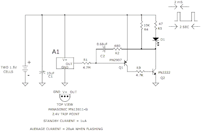
3v Low Battery Voltage Flasher

Many battery powered devices use two AA alkaline cells.  Often you will not know when it is time to replace the batteries until the device powered by them actually stops operating.  The hobby circuit below can be connected to a 3v battery, to give you some warning when the battery is nearing its end of life.

Circuit Project:3v Low Battery Voltage Flasher Circuit
 
It will flash a LED when the battery voltage drops to about 2.4 volts. The electronic circuit draws only 1ua of current in standby mode and jumps to only 20ua when flashing, so it can safely be included without depleting the battery energy. A voltage detector IC from Panasonic (Microchip also makes similar devices) is used to monitor the battery voltage. The device’s open drain output swings low, when the battery voltage is below 2.4 to 2.5 volts. This action turns on the two transistor oscillator circuit, which drives the LED with short current pulses lasting only 2ms.
Source: DiscoverCircuits
Read More..

Thursday, September 18, 2014

Low Cost Step Down Converter With Wide Input Voltage Range

The circuit described here is mostly aimed at development engineers who are looking for an economical step-down converter which offers a wide input voltage range. As a rule this type of circuit employs a step-down converter with integrated switching element. However, by using a more discrete solution it is possible to reduce the total cost of the step-down converter, especially when manufacturing in quantity. The TL5001A is a low-cost PWM controller which is ideal for this project. The input voltage range for the step-down converter described here is from 8 V to 30 V, with an output voltage of 5 V and a maximum output current of 1.5 A.


When the input voltage is applied the PWM output of IC1 is enabled, taking one end of the voltage divider formed by R1 and R2 to ground potential. The current through the voltage divider will then be at most 25 mA: this value is obtained by dividing the maximum input voltage (30 V) minus the saturation voltage of the output driver (2 V) by the total resistance of the voltage divider (1.1 kΩ). T1 and T3 together form an NPN/PNP driver stage to charge the gate capacitance of P-channel MOSFET T2 as quickly as possible, and then, at the turn-off point, discharge it again.

The base-emitter junction of T3 goes into a conducting state when the PWM output is active and a voltage is dropped across R2. T3 will then also conduct from collector to emitter and the gate capacitance of T2 will be discharged down to about 800 mV. The P-channel MOSFET will then conduct from drain to source. If the open-collector output of the controller is deactivated, a negligibly small current flows through resistor R2 and the base of T1 will be raised to the input voltage level. The base-emitter junction of T1 will then conduct and the gate capacitance of T2 will be charged up to the input voltage level through the collector and emitter of T1.

The P-channel MOSFET will then no longer conduct from drain to source. This driver circuit constructed from discrete components is very fast, giving very quick switch-over times. Diodes D2 and D3 provide voltage limiting for the P-channel MOSFET, whose maximum gate-source voltage is 20 V. If the Zener voltage of diode D2 is exceeded it starts to conduct; when the forward voltage of diode D3 is also exceeded, the two diodes together clamp the gate-source voltage to approximately 19 V. The switching frequency is set at approximately 100 kHz, which gives a good compromise between efficiency and component size.

Finally, a few notes on component selection. All resistors are 1/16 W, 1 %. Apart from electrolytic C1 all the capacitors are ceramic types. For the two larger values (C2 and C5) the following are used:
  • C2 is a Murata type GRM21BR71C105KA01 ceramic capacitor, 1 µF, 16 V, X7R, 10 %;
  • C5 is a Murata type GRM32ER60J476ME20 ceramic capacitor, 47 µF, 6.3 V, X5R, 10 %. D1 (Fairchild type MBRS340T3) is a 40 V/3 A Schottky diode. Coil L1 is a Würth WE-PD power choke type 744771147, 47 µH, 2.21 A, 75 mΩ.
  • T1 (BC846) and T3 (BC856) are 60 V, 200 mA, 310 mW complementary bipolar transistors from Vishay. The TL5001AID (IC1) is a low-cost PWM controller with an open-collector output from Texas Instruments.

Read More..

Tuesday, September 16, 2014

AD844 Low Distortion Amplifier Compressor

Designers can build a 15-dB compressor with a miniature lamp and a current-feedback amplifier. The circuit possesses extremely low distortion at frequencies above the lamp`s thermal time constant. This means that distortion is negligible from audio frequencies to beyond 10 MHz. There`s also relatively little change in phase versus gain compared to other automatic gain-control circuits. Lastly, the circuit has many instrumentation, audio, and high-frequency applications as a result of its low distortion and small phase change. The AD844 op amp is a perfect fit for this application because it`s a current-feedback amplifier. Each stage of the circuit, U2, lamp, and feedback resistor compresses an ac signal by over 15 dB (see the figure). Cascading a number of stages delivers higher compression ranges. Op amp U1 operates as a unity-gain buffer to drive the input to the compressor. However, U1 is optional if a low-impedance signal source is used. The lamp`s resistance will increase with temperature, which reduces the ratio of resistor R3 to the resistance of the lamp. This ratio reduces the gain of U2. The lamp`s cold resistance should be greater than the input resistance of U2 (more than 50 ) for proper operation. The lamp`s resistance will change slightly for low input levels. Therefore, the ratio of R3 to the resistance of the lamp and the gain of U2 stays high.

Read More..

Friday, September 12, 2014

Tone control low noise circuit

Tone control or pre-amplifier is an amplifier circuit supporters. Sometimes some of us do not know where a good amplifier, a raft alone and the results are not much different or even the same. Therefore we must know the character of the advantages and disadvantages of each amplifier equipment.

Tone control low noise here does not mean without noise, but noise compared with the lowest tone control on the market, for example Ronica transistor 4, TL-084, TC-2 LM833 etc.

CSE | Circuit Schematic Electronics

Jump toexplanation of each component ...

Potensio 1 serves to regulate the intensity / level of the incoming signal is assisted potensio 2 as balance / counterbalance. Potensio 2 is still installed and is usually an optional component. 1-2uF/250V capacitor R1 is actually a brand name,but I prefer to replace it with a 1K resistor / 5% normal for reasons to avoid hum and interference sensitive. R2 R3 while minimizing interruption to adjust the impedance OP-amp 1. R4 and R5 serves to increase the gain of 1.3 times. Pre amplifiers typically use a strengthening standards by 2 times, but by most of us think it has a noise. So I chose the value of 1.3 times, but the most minimal noise signal from the volume is enough to make the lamp light peak.

For low noise ...Cause of noise in op amp 1, apex audio even eliminate this stage. CanThis step is also used as a buffer (jumper R5), the strengthening of a time. Lower values ​​increase the value of R5 or R4 with consequent gains to be less, but remains at a value above 1 times due to input non-inverting path to take, so that the signal and noise can be reduced. R4 can also be replaced with a 10K trimpot and middle leg into the bass range adjuster (bass resonance).

C1 and C6 as a filter to reduce the treble / high frequency of excessive or often called oscillation prevention. R6 is actually an optional component of the impedance a little help customize the system. Ideally the same as the R8 R7 to facilitategive the sign of the gain on potensio panel tone control. C2 and C3 form a series circuit treble filter (high pass filter), its value is greater then the sound that passed the mid. C4 and C5 assisted by R9 and R10 form the low pass filter (filter bass), the greater the value of C is a bass sound that will be missedthe soft / low (maximum of 47nF), the smaller the value of c is the bass signal that is passed will further dip (dig-dig, c4 = c5 = 22nF). This value is suitable for 27-33nF, 47nF instead (depending on taste). Pot 3 & 4 pot set treble and bass levels, the greater the greater the value of this potensio gains (bass & treble including potensio volume). R11 adjusts the output impedance, while the R12 and the red LED indicator that shows if the amplifier Peak has been given a full signal.

15V maximum supply. TL074 IC can, but in designing the PCB, IC can bereplaced with 2x TL072/NE5532/4558.
Read More..

Low Power Voltage Doubler Wiring diagram Schematic

All miniature electronic devices operate off batteries. Some of them need higher than the standard battery voltages to operate efficiently. If the battery of that specific voltage is unavailable, we are forced to connect additional cells in series to step up the DC voltage. Thus, the true meaning of miniaturisation is lost. A simple way to overcome this problem is to employ a voltage doubler, if the device under consideration can operate at a small current.

Here we present a low-power voltage doubler schema that can be readily used with devices that demand higher voltage than that of a standard battery but low operating current to work with. The schema is quite simple as it uses only a few components. Yet, the output efficiency is 75 to 85 percent along its operating voltage range. The available battery voltage is almost doubled at the output of the schema.

Here IC1 is wired as an astable multivibrator to generate rectangular pulses at around 10 kHz. This frequency and duty cycle of the pulses can be varied using preset VR1. The pulses are applied to switching transistors T1 and T2 for driving the output section, which is configured as a voltage-doubling schema. The doubled voltage is available across capacitor C5. During each cycle of the pulse occurance, the high level drives T1 into its saturation, keeping transistor T2 cut off.


Low-Power Voltage Doubler Circuit Diagram

So transistor T1 charges capacitor C4 via the path formed by diodes D2 and D1 to a voltage level slightly lesser than the supply. But during the low period of the pulse, transistor T1 is cut off while transistor T2 is driven into saturation. Now, transistor T2 raises the charge on the negative pole of capacitor C4 by another step equal to the supply voltage. Therefore an equal amount of charging is built up on capacitor C5 via diode D3.

This doubling action increases the total voltage across capacitor C5 to almost double the input voltage. If the output of the pulse generator is maintained with a high enough amplitude and frequency, the output voltage and current remain constant and cater to the needs of the load. Even with the half-wave function, this schema is almost free of ripple voltage. If the connected load doesn’t require a high current, the efficiency can be expected in the upper 90 percentranges.

Since the input voltage is doubled, the current drain from the input power supply is also doubled at the input but halved at the output. One point of caution is that if the multivibrator’s frequency is fairly high, the output may suffer with the interference imposed over the DC voltage. In this case, the frequency must be set favorably by trials and actual load connection procedure. This tiny schema can be assembled on the general-purpose PCB. If all of the components are surface-mount type, the whole module can be genuinely miniaturized.

EFY Lab note. During testing with input of 8V and 1.25mA load current the output voltage was found to be around 13V.

Author :M.K. Chandra ,Mouleeswaran And A.N. Vadivudai Naayaki
Source :efymag
Read More..