There are two types of coupling between electronic circuits:
AC coupling means that only the AC parts of the signal will pass. For this normally a capacitor is used that connects the two circuits. The minimum value of the capacitor depends upon the lowest frequency (f) that has to be transmitted and the input/output impedance (R) of the two circuits. The approximate formula for the minimum capacity is C ~ 1/(R*f) with f = lowest frequency, R = in/output resistance Example: minimum frequency = 50Hz, in/output resistance = 10kOhm -> C ~ 2 uF (u = micro = 1/1000000). A usual value would be 2.2uF in this example. AC coupling is normally used for audio signals. For audio signals AC coupling has the advantage that unwanted DC shares in the signal are removed. For some AC processing circuits (e.g. amplifiers, filters) DC voltages are not allowed in the input signal. Therefore very often a capacitor can be found in the input stage of such circuits. DC coupling means that both DC and AC parts of a signal are transmitted. For control voltages (normally) only DC coupling can be used as even fixed voltages (e.g. coming from a manual control) have to be transmitted. In a module patch each A-100 module can be treated as an electronic circuit that is connected to another one. Consequently one has to take into consideration the type of coupling (AC or DC) between modules as the strict differentiation between AC and DC applications os softened for some A-100 modules. E.g. a VCA can be used to process audio signals (i.e. normally AC coupled signals) as well as slowly changing CV voltages (e.g. envelope or modulation amount). Therefore one needs to know if a VCA used is AC or DC coupled. Another example is a divider (e.g. A-115 or A-163) as even these module can be used to process audio or (slow) clock/gate signals. | |
 | Luckily it is not very complicated to switch between AC and DC coupling. All one has to do is to bride (i.e. short circuit) the capacitor in case of an AC coupled in/output. The left picture shows how the switch is connected in parallel to the AC coupling capacitor (the broken line resistor symbol represents the load to GND that is always available in each circuit as reference to GND). If AC coupling is required for a DC coupled in/output simply a capacitor has to be added. From the schematics it can be seen if an in/output is AC or DC coupled. We will add this information also to the users manual for modules that may be used for both types of coupling. For some circuits resp. modules changing from AC to DC coupling is not possible. E.g. the "old" VCAs A-130 and A-131 (those with CEM3381 or CEM3382) are AC coupled as the special CEM circuits cannot be DC coupled because of the internal negative reference voltage. The "new" VCAs A-130 and A-131 (those with CA3080) are DC coupled and can be used to process CV signals too. A list with the type of coupling for all modules in question will follow soon. For most of the modules the question about the type of coupling does not arise. E.g. all filters are AC coupled and all CV generating and processing modules (e.g. ADSR, LFO, slew limiter, Theremin, Ribbon controller, random voltage) are DC coupled. But for other modules the type of coupling is not obvious (e.g. VCA, divider, waveshaper). |
Wednesday, September 24, 2014
PCM2902 Soundcard with Microphone Input Schematic

PCM2902 Soundcard with Microphone Input Schematic
Many of us have a pair of headphones connected to the output of the computer sound card us either to enjoy songs, or a game. Very likely your headphones and microphone, which also connect to the appropriate slot your sound card. But at some point broke down the female plug my sound card, and because quite a lot to change the plug when I put the headphones and when the speakers. A small structure is a sound card, USB, with stereo inputs / outputs, button to increase / volume button for volume and mute! When connected Windows will recognize as a sound card! With all the materials to be SMD, the cornered enough and fit into a small plastic box, which by one measure has a cable with USB plug, sound to go acoustic (Left / Right) and condenser microphones.
The supply of (as imagined) is done by the USB port. The heart of the integrated circuit is PCM2902 of Burr-Brown by Texas Instruments. It is stereo 16-bit DAC and ADC, fully compatible with USB 1.1. DAC sampling frequencies are 32, 44.1 and 48 kHz, ADC has 8, 11.025, 16, 22.05, 32, 44.1 and 48 kHz. If you want more sound intensity, you will need to connect TDA 7050 amplifier to audio output.
Tuesday, September 23, 2014
Adjustment power supply values 1 25 15V Max current 0 5 amp circuit

This is power supply that have Voltage output fine the value has 1.25-15V. From by Output current that be valuable about 0.5 amp that 12V and 0.2 amp that 15V.
When Volt , from 220V houses reach transformer. It will modify Volt 220V to be 18VAC already to change rectifier circuit. Which D1, D2, C1 and R1 wasp be Full wave rectifier circuit. For modify DCV to ACV to a signal DCV. It make get a signal DCV that have voltage at pin 3 of IC1 be 20V. From that time DCV signal this reach fight DC Regulator circuit. Which use IC number LM317.
This circuit will perform to maintain one’s position Voltage smoothly. Which level output voltage at get this will go out the way pin 2 of IC1. By have capacitors C2 be voltage filter in order that voltage output level of the circuit is will high class modify to follow fining. The performing fee withstands VR1 there.
from:eleccircuit.com
Adjustable voltage output control by 2SC458

The principle works be transistor Q1 2SC458 that built model common-emitter amplifier, which perform fine decrease input voltage get down then heal volt that give may but at collector voltage compare with ground. Which get from the combination of voltage at base – emitter pin (0.6V) with VZener diode (6.2V) already fine the value of a resister can fine the value VR1 help transistor part Q2 2SC458 perform be compared as power supply current source and current that fixed. By current at flow come in the way base pin of Q2 and when Q2 bias current. That already Voltage output get, with fining that a resister VR1 during 5.8V-15.8V. By have R3 and C1 perform be RC Filter caution. This circuit power current source get 100mA topmost should apply to load that use current low.
s:www.eleccircuit.com
DTMF Remote Control RC Radio Circuit
Here is a remote control (RC) radio unit circuit which makes use of the radio frequency signals to control various electrical appliances. This remote control unit has 4 channels which can be easily extended to 12. This RC circuit differs from similar circuits in view of its simplicity and a totally different concept of generating the control signals.
Here we make use of DTMF (dual-tone multi frequency) signals (used in telephones to dial the digits) as the control codes. The DTMF tones are used for frequency modulation of the carrier. At the receiver unit, these frequency modulated signals are intercepted to obtain DTMF tones at the speaker terminals.
Remote Control Radio Circuit Schematic
The remote control transmitter consists of DTMF generator and an FM transmitter circuit. For generating the DTMF frequencies, a dedicated IC UM91214B (which is used as a dialler IC in telephone instruments) is used here. This IC requires 3 volts for its operation. This is provided by a simple zener diode voltage regulator which converts 9 volts into 3 volts for use by this IC.
Rest of the pins of this IC may be left as they are. The output of IC1 is given to the input of this transmitter circuit which effectively frequency modulates the carrier and transmits it in the air. The carrier frequency is determined by coil L1 and trimmer capacitor VC1 (which may be adjusted for around 100 MHz operation). An antenna of 10 to 15 cms (4 to 6 inches) length will be sufficient to provide adequate range.
The antenna is also necessary because the transmitter unit has to be housed in a metallic cabinet to protect the frequency drift caused due to stray EM fields. Four key switches (DPST push-to-on spring loaded) are required to transmit the desired DTMF tones. The switches when pressed generate the specific tone pairs as well as provide power to the transmitter circuit simultaneously. This way when the transmitter unit is not in use it consumes no power at all and the battery lasts much longer.
The receiver unit consists of an FM receiver (these days simple and inexpensive FM kits are readily available in the market which work exceptionally well), a DTMF-to-BCD converter and a flip-flop toggling latch section. The frequency modulated DTMF signals are received by the FM receiver and the output (DTMF tones) are fed to the dedicated IC KT3170 which is a DTMF-to-BCD converter.
Simple Class A Power Amplifier by IRF530
I was in need of high quality headphones amplifier because of many reasons and decided to build SDS Labs phone amp. This is extremely rewarding project in a sense that it is fully documented, includes PCB, parts list and building notes – so it’s easy to build and then it sounds great.
I have used IRF530 and IRF9530 pairs and they work just fine given the fact that you add 100-300 Ohm gate resistors to prevent high frequency oscillations. This is a common problem for MOSFET designs and if you don’t have a good oscilloscope or want to be on the safe side just use gate resistors on any MOSFET design. Ferrite beads put over gate pin could also be used instead but I somehow prefer resistors.
Monday, September 22, 2014
Changing between AC and DC coupling
Changing between AC and DC coupling
Class A Power Amplifier by IRF530N 78L05
This is the best design I have came up so far!
I use two 6x6x4cm heatsinks per channel. Power supply is unregulated (just transformer, diode bridge and capacitors) but I cannot hear anything even when I put my ear within few centimeters of the loudspeaker. Opamp has very good power supply rejection ratio. I’ve tried to keep everything as simple as possible and basically LM317 would be just one extra opamp
If you are looking for better sound, get separate regulated low power supply just for the U1 opamp, something like +-15V at 100-200 mA.
I have also used one LM7805 to get bias for both channels – you may want to use two separate 7805 in a final amp to get better channel separation. R2 pot is anything from 500 to 50k. I have used 22k.
Create natural sound using ic MM5837
Normal voice we hear is from frequencies that are a combination of both high frequency and low frequency. Signal strength is not equal, will result in a different voice.
Operation of the circuit. When the power supply to IC1 by IC1 will work out the frequency produced by the pin 13 pin 3 is press the switch on left off. C to a value that will be connected to each circuit by the C makes the sound different.
Of the signal from pin 3 of IC1 is through R1 and VR1 is responsible for adjusting the strength of the signal will be expanded to IC2, which IC2 is IC amplifier with growing 1W signal that originates in the leg 5. The high frequency. And noise will be R3, C8 filter to ground the remaining signal is Retail Oil Link to C9 on the speakers.
Horn siren use the IT and OT transformer
Basically siren on a police patrol car and an ambulance use electronic circuit connected to the DC current. When the switch is pressed, the siren sounds immediately come out.For those of you who own a car, or any motor you can also create a similar horn. Placement was also very practical. And if you want the flashing lights can add your own. In a series of above do not use flashing lights as the sirens sound.

R1 = 47K
R2 = 200R
C1 = 0,02uF
C2 = 50uF 16V
C3 = 0,005uF
T1 = 2SB178 PNP transistor
S1 = Push button switch
G1 = 6-12V battery
TR1 , IT transformer is reversed. used a two-legged.
TR2 , OT output transformer OT240
How to use it is to put the above series into a box. Adjust the size to be more practical. Then insert the cable of a car or motorcycle battery voltage as described above that is 6-12 V battery into the plug. In accordance with their respective poles.Three feet of IT transformer wrapped so as not to stick to the body of the car or motorcycle. Cover with insulation that is resistant to water. Then try if already issued a siren sounds and if so, ready for use.
With Time Delay High And Low Voltage Cut Off
Overview
The power line fluctuations and cut-offs cause damages to electrical appliances connected to the line. It is more serious in the case of domestic appliances like fridge and air conditioners. If a fridge is operated on low voltage, excessive current flows through the motor, which heats up, and get damaged.
The under/over voltage protection circuit with time delay presented here is a low cost and reliable circuit for protecting such equipments from damages. Whenever the power line is switched on it gets connected to the appliance only after a delay of a fixed time. If there is hi/low fluctuations beyond sets limits the appliance get disconnected. The system tries to connect the power back after the specific time delay, the delay being counted from the time of disconnection. If the power down time (time for which the voltage is beyond limits) is less than the delay time, the power resumes after the delay: If it is equal or more, then the power resumes directly.
This circuit has been designed, built and evaluated by me to use as a protector for my home refrigerator. This is designed around readily available semi-conductor devices such as standard bipolar medium power NPN transistor (D313/SL100/C1061), an 8-pin type 741 op-amp and NE555 timer IC. Its salient feature is that no relay hunting is employed. This draw back is commonly found in the proctors available in the market.
The complete circuit is consisting of various stages. They are: - Dual rail power supply, Reference voltage source, Voltage comparators for hi/low cut offs, Time delay stage and Relay driver stage. Lets now look at the step-by-step design details.
Dual rail power supply.
This is a conventional type of power supply as shown in Figure 1. The power is applied through the step-down transformer (230/12-0-12V/500mA). The DC proportional to the charging input voltage is obtained from bridge rectifier. Two electrolytics are there to bypass any spikes present. Bridge is capable of handling currents up to 1 Amp.
Output is given by: -
V(out) = 0.71 X V (secondary)
= 0.71 X 24V
= 17.04 V
(This equation is similar for the negative rail as well)
Circuit diagram

Low voltage cut off op-amp
Figure 2 shows the use of very common and easily available op-amp 741 as a comparator. The op-amp is available in TO-5 and DIP type packing.
Circuit diagram
In this ckt the zener diode D1 and it’s associated resistor R1 are connected to the non-inverting terminal (+ve) of 741 to give the suitable reference voltage. The DC voltage from the sensor is given to the inverting (-ve) terminal through pre-set R2.This is used to set the input level.
When the sensor input is less than Zener voltage the output from the Op-amp remains high and when it is greater than Zener voltage the output goes low. When the sensing voltage is equal to Zener voltage the output of the op-amp is approximately zero.
This phenomenon is used as a decision for switching the relay and to give cutoff in a low voltage situation.
High voltage cut off op-amp
Here the op-amp is used as a inverted amplifier. See Figure 3.Zener and resistor network gives reference voltage to the inverting terminal (-ve) of op-amp. Sensing voltage derived through the 10 K pre-set is given to the non- inverting (+ve) terminal and this sets the high level cut.
When the input DC from the sensor is less than Zener voltage the output of the op-amp is low and vice-versa. When the input DC voltage is equal to the zener voltage, the op-amps output is approximately zero.
Circuit diagram
Time delay
I’ve selected the 555 timer due to following reasons.
1. Timing from microseconds through hours.
2. Ability to operate from wide range of supply voltages.
3. High temperature stability.
4. Easily Available.
5. Its triggering circuit is quite sensitive.
This is basically a monostable. The external timing capacitor C2 is held initially discharged by the timer. The circuit triggers upon receiving a pulse to its pin 2 when the level reaches 1/3 Vcc. Once triggered., the circuit will remain in that state until the set time is elapsed or power to the circuit cuts off. The delayed period in seconds is 1.1 C2.R1 where R1 is in megohms and C2 is in microfarads. In practice, R1 should not exceed 20 M. If you use an electrolytic capacitor for C2, select a unit for low leakage. The time delay may have to be adjusted by varying R1 to compensate for the wide tolerance of electrolytics.
Circuit diagram
Relay Driver
The output from the voltage level detectors cannot directly drive the relay and hence the relay driver is used.
Circuit diagram
The Complete Circuit
Circuit diagram
Under normal operating conditions i.e. when the input voltage is between maximum and minimum limit the output from the both the comparators are low. The transistor Q1 is OFF and the relay is in de-energized (pole connected to N/C pin) state and the output is obtained.
When the input voltage is below or above the limits set by the pre-sets R8 or R9, the output of the Op-Amps goes either low or high and diodes D1 or D2 would be forward biased depending on the situation. Transistor Q1 switches ON and the flow of current from collector to emitter energizes the relay and the output is cutoff.
A small amount of hystersis has been added via feed back resistors R10 & R11 so that the relay turns on when the level falls to a particular value but does not turn again until it raises a substantial amount above this value. Other wise the relay contacts will frequently turn on/off and produce chattering.
Construction Hints
1) I used a piece of varoboard, which has copper strips on one side to mount the components, and housed the entire circuit and the transformer in a discarded ATX PC power supply box.
2) An autotransformer has been used to set the limits. Set the output of the autotransformer to 250V AC and connect it to the primary of transformer T1 (see Figure 1). Then adjust the pre-set R9 such that relay just energizes. This is the high limit. Next set the output of the autotransformer to 200V AC and adjust the pre-set R8 such that the relay energizes. Please note that these are my preferred limits but you may select any range from say 170 to 270V AC.
3) A neon with a suitable resistor could be connected between the AC supply lines as an ON indicator. Alternatively, LED with a current limiting resistor could be connected between the relay coil so when the relay is energized LED will indicate the situation.
Car Battery Charger description and circuit diagram
This charger will quickly and easily charge most any lead acid battery. The charger delivers full current until the current drawn by the battery falls to 150 mA. At this time, a lower voltage is applied to finish off and keep from over charging. When the battery is fully charged, the circuit switches off and lights a LED, telling you that the cycle has finished.
Circuit diagram
Parts
R1 500 Ohm 1/4 W Resistor
R2 3K 1/4 W Resistor
R3 1K 1/4 W Resistor
R4 15 Ohm 1/4 W Resistor
R5 230 Ohm 1/4 W Resistor
R6 15K 1/4 W Resistor
R7 0.2 Ohm 10 W Resistor
C1 0.1uF 25V Ceramic Capacitor
C2 1uF 25V Electrolytic Capacitor
C31000pF 25V Ceramic Capacitor
D1 1N457 Diode
Q1 2N2905 PNP Transistor
U1 LM350 Regulator
U2 LM301A Op Amp
S1Normally Open Push Button Switch
MISC Wire, Board, Heatsink For U1, Case, Binding Posts or Alligator Clips For Output
Notes
1. The circuit was meant to be powered by a power supply, which is why there is no transformer, rectifier, or filter capacitors on the schematic. There is no reason why you cannot add these.
2. A heatsink will be needed for U1.
3. To use the circuit, hook it up to a power supply/plug it in. Then, connect the battery to be charged to the output terminals. All you have to do now is push S1 (the "Start" switch), and wait for the circuit to finish.
4. If you want to use the charger without having to provide an external power supply, use the following circuit.

C1 6800uF 25V Electrolytic Capcitor
T1 3A 15V Transformer
BR1 5A 50V Bridge Rectifier 10A 50V Bridge Rectifier
S1 5A SPST Switch
F1 4A 250V Fuse
5. The first time you use the circuit, you should check up on it every once and a while to make sure that it is working properly and the battery is not being over charged.
Sunday, September 21, 2014
Laptop Power Supply for Car 95W
Laptop Power Supply for Car 95W Laptop Power Supply Module A laptop or notebook computer user while they are away from the home or office knows that
 A laptop or notebook computer user while they are away from the home or office knows that sooner or later they will need to plug into a mains outlet to top up the batteries. The car cigarette lighter socket in the car is also an electrical outlet but it can only supply 12 V. That’s no problem for the Laptop Power Supply described here.
The laptop power supply described here plugs into a car cigarette lighter socket and produces a 19V nominal output voltage adjustable by + - 0.5V. The input voltage range is from 9.2V to 15V and the output voltage shows good regulation even with large fluctuations of the input voltage. The output can supply 5A continuosly with brief excursions up to 10A.
The power semiconductor heatsinks of this laptop power supply are dimensioned fo 5A continuous so extended operation up to 10A will increase dissipation in the adapter and in extreme cases will cause the input fuse to complain.
Laptop PSU Adaptor Parts List
Resistors:
R1 = 5k6
R2 = 51k (51k1)
R3 = 9k1 (9k1)
R4 = 1M
R5 = 4k7
R6,R8 = 15k
R7 = 27k
R9,R10 = 6,8
R11 = 10k
R12 = 100
P1 = 5k preset
Capacitors:
C1-C4 = 3300µF 16V, radial, low ESR, diam. 12.5 mm, e.g. Panasonic EEUFC1C332 (Farnell)
C5,C10 = 1µF MKT, lead pitch 5mm or 7.5mm (larger version preferred)
C12 = 1µF MKT, lead pitch 5 mm
C6-C9 = 2200µF 25V radial, low ESR, diam. 12.5mm, e.g., EEUFC1E222 (Farnell)
C11 = 22nF, lead pitch 5mm
C13 = 2nF2, lead pitch 5mm
C14,C15 = 100nF ceramic, lead pitch 5mm
C16 = 10µF 63V radial
Inductors:
L1 = 56µH, 21 turns 10 x 0.5 mm ECW, parallel
1 x ETD 29 coil forner, vertical mounting, Epcos B66359X1014T1 (Schuricht # 331622)
2 x ETD 29 clamp, Epcos B66359-A2000 (Schuricht # 333862)
2 x ETD 29 core half, material # N67, air gap 0.5mm, Epcos B66358-G500-X167 (Schuricht # 333840)
Semiconductors:
D1 = MBR1645 (International Rectifier) (e.g. Reichelt, Segor)
T1 = IRL2505 (International Rectifier) TO-220AB case, (e.g., RS Components)
T2 = BD139
T3 = BD140
IC1 = UC3843N (Texas Instruments) (e.g. Reichelt, Segor)
Miscellaneous:
K1-K4 = 2-way spade terminal, vertical, PCB mount
F1 = fuse, 10A/T (slow) 6.3 x 32 mm (¼ x 1¼ inch) + 2 fuse holders for 6.3 mm diameter and PCB mounting
2 x heatsink type SK104-STC (or STS) TO220 38.1mm, 11K/W (Fischer Electronic) Isolating washers for T1 and D1 (TO-220AB) + isolating bushes
PCB
Laptop PSU Adaptor PCB-Layout


Source: Laptop Power Supply Adaptor 95W
Thermistor Temperature Monitor Circuit and explanation
Thermistor Temperature Monitor Circuit and explanation

This sensor circuit uses an ordinary NTC thermistor with a resistance of 47k at room temperature. A suitable part from Maplin Electronics is FX42V. The circuit is set in balance by adjusting the the 47k potentiometer. Any change in temperature will alter the balance of the circuit, the output of the op-amp will change and energize the relay. Swapping the position of the thermistor and 47k resistor makes a cold or frost alarm.

At room temperature (25 degrees Celsius) a 47k NTC thermistor resistance is approximately 47k. The non-inverting op-amp input will then be roughly half the supply voltage, adjusting the 47k pot should allow the relay to close or remain open. To calibrate the device, the thermistor ideally needs to be at the required operating temperature. If this is for example, a hot water tank, then the resistance will decrease, one way to do this is use a multimeter on the resistance scale, read the thermistors resistance and then set the preset so that the circuit triggers at this temperature.
Please note that if the temperature then falls, the relay will de-energize. If the environment temperatures changes rapidly, then the relay may chatter, as there is no hysteresis in this circuit.
Hysteresis, allows a small amount of "backlash" to be tolerated. With a circuit employing hysteresis, there will be no relay chatter andthe circuit will trigger at a defined temperature and require a different temperature to return to the normal state. Hysteresis can be applied to the circuit using feedback, try a 1 Mega resistor between op-amp output, pin 6 and the non-inverting input pin 2 to give the circuit hysteresis.
Without offset null adjustment, the output of the 741 IC will be around 2 Volts (quiescent) swinging to nearly full supply when triggered. The 4.7k and 1k resistor form a potential divder so that under quiescent conditions the transistor will be off. Quiescent or steady state means no signal, or in this case (when the temperature does not cause the output to swing to full voltage).
Source: Temperature Monitor
30V Variable Power Supply Using LM317
Circuit diagram

Electric Guitar Violin Preamplifier
This is generated by a voltage divider comprising two 10kΩ resistors and bypassed by a 47µF capacitor to reject noise and hum. IC1a is configured as a non-inverting amplifier with a gain of between 2 and 20, depending on the setting of VR1. IC1a’s output is fed to VR2 via a 22µF capacitor, allowing the output volume to be set. The audio then passes to the non-inverting inputs of the remaining three op amps (IC1b-IC1d) which are connected in parallel to provide a low output impedance; it will drive a load impedance as low as 600Ω. The 100Ω resistors in series with the outputs provide short-circuit protection for the op amps and also prevent large currents from flowing between the outputs in case they have slightly different offset voltages.
 The buffered signal is then AC-coupled to two output connectors using 47µF electrolytic capacitors. For Output 1, a 47kΩ resistor sets the output DC level to ground and a 220Ω series resistor provides further short-circuit protection. Output 2 is similar but includes another potentiometer (VR3) to allow its level to be set individually. Note that this means the impedance of Output 2 can be high (up to 2.5kΩ depending on the position of VR3’s wiper). The total harmonic distortion of this circuit is typically less than 0.01% with the gain set to six. If a TL064 is used instead of a TL074, the current drain will decrease but there will be more noise at the output. Finally, the input impedance can be increased by increasing the value of the 330kΩ resistor to suit high-impedance pick-ups.
 Fuse Box Toyota 2000 MR2 Spyder Passenger Compartment Diagram
Fuse Box Toyota 2000 MR2 Spyder Passenger Compartment Diagram


Fuse Panel Layout Diagram Parts: stop lamp, tail light, power window, radio, dome light, ECU, fuse panel, radio, cigar lighter, washer, heater, wiper, ignition coil, ignition fan, turn lamp, gauge, ACC, SRS, window defogger, door lock, fog lamp.
Generic Amplifier
 |
| Generic Amplifier |
do it yourself DIY Speaker Project Perfect Sound Granite
Speaker Project Summary
External box dimensions 240 x 350 x 280 mm. Internal box dimensions 200 x 310 x 240 mm. Box material 20 mm thick black granite (Nero Assoluto). Weight 35 kg.
Enclosure volume 14.9 L. Bass reflex enclosure tuned to 45 Hz. Port length 160 mm
Input power 80W. Sensitivity 87.5 dB. Transmission bandwidth 40Hz - 20kHz. Impedance 6 ohm.
Seas Loudspeaker Drivers
The drivers selected for this loudspeaker system are from Seas who has been producing speaker drivers for over 50 years. The tweeter is the Seas 27 TFFC which has a fabric dome. The Sonolex lightweight fabric dome has high consistency and provides excellent stability against variations in air humidity. The stiff and stable rear chamber allows for a moderately low crossover frequency (~2500kHz). This made the Seas 27 TFFC tweeter the right choice for our granite loudspeaker project.
The woofer we used is the Seas G17REX/P. The woofer consists of a fiber glass cone, a bullet shaped phase plug and a high loss rubber surround. These are carefully matched to each other resulting in smooth frequency response.
Speaker Box and Crossover Design
The speaker box and crossover network were designed by M.Janura and K.Sýkory using the LspCAD speaker design software package. A volume of 15L (dimensions 220 x 350 x 250 mm) and a tuning frequency of 45 Hz was used for the speaker box. The dividing frequency is 2.5kHz and the drivers are connected in phase. The crossover schematic and modeled frequency response are shown below.

The components used in the crossover dividing network are from TESLA. I think that the people in the former Czechoslovakia were able to produce high quality components, but you may use your favorite type. The condensers (capacitors) used in crossover are MKT type - we did not use bipolar condensers because they have disadvantages that I wont further specify. The inductors are air core.
Sound
I was knocked off my feet with the sound after the first track we played: Everlast - Folsom Prison Blues by the legendary Johnny Cash. The song tested bass response of the speakers. We didnt expect such deep and accurate bass from small speakers. The speakers deliver very detailed sound (soft treble and great imaging). They play rock music aggressively and classical music with emotion. As we say: "they play like HONEY" (it means - brilliant) and they look great too.
I would like to thank to Marian Mózer and everyone in the team for their effort and for the job well done. The loudspeaker system is designed by M.Janura and K.Sýkory - named Besie 1.
We understand that most of you will not be able to make speaker boxes of granite. If you are interested in speakers made from granite, please send me an email and we may be able to help you. Thank you and I hope you enjoyed our project.
Audio Amplifier 1000W
Amplifier description:
Amplifier circuit diagram:

Amplifier circuit diagram:

Explanation Fuse Box Chevrolet Suburban Engine 1993 Diagram
Fuse Box Chevrolet Suburban Engine 1993 Diagram

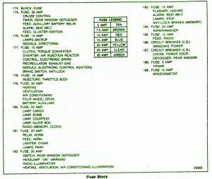
Fuse Panel Layout Diagram Parts: cruise control, rear window defogger, auxilliary battery relay, alarm seat belt, cluster ignition, lamps back up, clutch, air injection reactor, control electronic park, recirculator exhaust gas, module electronic control ignition, brake switch, injector, throttle body, heating, ventilation, air conditioning, four wheel drive, battery auxilliary, lamp cargo, lamp dome, courtesy lamp, glove box, radio, horn relay, feed relay, park lamp, rear window defogger, headlamp, radio illumination, heating ventilation, hazard alarm, seat belt lamps, wiper, washer, power window, power door lock.
Saturday, September 20, 2014
5 Watt Class A Audio Amplifier Circuit diagram
5 Watt Class-A Audio Amplifier Circuit diagram
Parts:
P1 = 47K
R1 = 100K
R2 = 12K
R3 = 47K
R4 = 8.2K
R5 = 1.5K
R6 = 2.7K
R7 = 100R
R8 = 100R
R9 = 560R-1/2W
R10 = 1R-1/2W
Q1 = BC560
Q2 = BD439
Q3 = BD439
C1 = 10uF-63V
C2 = 10uF-63V
C3 = 47uF-25V
C4 = 100uF-35V
C5 = 150nF-63V
C6 = 220uF-25V
C7 = 220uF-25V
C8 = 1000uF-25V
SPKR = 5W-8R Speaker
Notes:
- If necessary, R2 can be adjusted to obtain 13V across C8 positive lead and negative ground.
- Total current drawing of the schema, best measured by inserting the probes of an Avo-meter across the positive output of the power supply and the positive rail input of the amplifier, must be 700mA. Adjust R8 to obtain this value if necessary.
- Q2 and Q3 must be mounted on a finned Heatsink of 120x50x25mm. Minimum dimensions.
- Add R5 and C5 if the bass-boost facility is required.
Fuse Box Diagram Of 2002 Kia Optima
 |
| Fuse Box Diagram Of 2002 Kia Optima |
88 108 MHz FM Broadcast Transmitter
Fine adjustment can often be done by adjusting the 200 Ohm resistor in series with the battery. Oscillator frequency is set by an inducer of turn 5 and 13 pF capacitor operated. The inductor is wound around a # 8 x 32 bolt (about 3 / 16 in diameter) and then removed by unscrewing the screw. The inductor was then streached to about a length of 3 / 8 inches and hit near the center. The oscillator frequency should come out somewhere near the center of the band (98 MHz) and can be moved up or down slightly the expansion or compression of the coil.
A small signal diode (1N914 or 1N4148) is used as a varactor diode so that the total capacity in parallel with the coil varies slightly in the type of audio causing the oscillator frequency to change the audio rate (600 Hz) . The ramp waveform at pins 2 and 6 of timer applies to the reverse diode across a large bias (1 Meg) resistor so that the capacity of the diode changes as voltage changes thus increasing altering the frequency of tank circuit.
Alternatively, an audio signal could be applied to the 1 Meg resistor to modulate the oscillator but may require a pull-up resistor to reverse bias additional diode. The N channel JFET transistors used should be high frequency VHF or UHF types (Radio Shack # 276-2062 MPF102) or similar.
Build a 500W low cost 12V to 220V Inverter Circuit Diagram
500W low cost 12V to 220V Inverter Circuit Diagram
How to calculate transformer rating
The basic formula is P=VI and between input output of the transformer we have Power input = Power output
For example if we want a 220W output at 220V then we need 1A at the output. Then at the input we must have at least 18.3V at 12V because: 12V*18.3 = 220v*1
So you have to wind the step up transformer 12v to 220v but input winding must be capable to bear 20A.
Attention: This Circuit is using high voltage that is lethal. Please take appropriate precautions
Audio Amplifier 10W TDA1042
- VCC MIN. V - 9
- VCC NOM. V - 9
- VCC MAX. V - 18
- P. OUT W - 10
- RL OHM - 2
 |
| Audio Amplifier 10W TDA1042 |
Fuse Box Toyota 2009 Camry LE Diagram
Fuse Box Toyota 2009 Camry LE Diagram


Fuse Panel Layout Diagram Parts: fog light switch, turn signal switch, dimer switch, light control switch, headlight dimmer switch, gauge fuse, parking brake switch, stop light switch, turn signal flasher assembly, instrument panel, main body, ignition relay, ACC relay, tail relay, fog relay, tail light fuse, stop lamp fuse, fog lamp fuse, automatic light control sensorm ignition key cylinder, hazard warning switch,.
Fuse Box Ford 1990 Thunderbird Super Coupe Diagram
Fuse Box Ford 1990 Thunderbird Super Coupe Diagram


Fuse Panel Layout Diagram Parts: rear window defroster, anti lock motor, fuse panel, headlamp, passive restraints, ignition coil, powertrain control module, fuel pump motor, auto shock, ignition switch, blower motor, anti lock module, horn, hazard, memory.
Stepped Volume Control
Circuit diagram:

The counter state determines the configuration of the four electronic switches inside the 4066 and so the series resistance effectively seen in the audio signal line. The circuit should be powered from a 9-V regulated supply or a battery and will consume a few milliamps only. Switch S1 allows the counter to be reset, switching all 4066 switches to off, i.e., the highest attenuation will exist in the audio path as in that case none of the 1-kΩ resistors are shorted out. To calibrate the circuit, disconnect the 4040 clock input (pin 10) from the wiper of P1, and temporarily ground it through a 100 kΩ resistor. Now pulse the clock input by briefly connecting it to the +9 V line; you will see the counter outputs change state and with them, the bilateral switches in the 4066.
Friday, September 19, 2014
100W LM3886 Parallel Stereo Power Amplifier
The LM3886 circuit is in a non-inverted configuration, so the input impedance is determined by the input resistor R1, i.e. 47k. The 680 ohm and 470pF resistor capacitor filter network is used to filter out the high frequency noise at the RCA input. The 220pF C4 and C8 capacitors are used to shot out the high frequency noise at the LM3886 input pins. I used high quality audio grade capacitors at several locations: 1uF Auricap at the input for DC blocking, 100uF Blackgate for C2 and C6, and 1000uF Blackgate at the supply filter.

Finished PCB.
The 20k and 1k resistors are hand matched to 0.1%. For the output resistors, I used six 0.5W 1% 1ohm resistors in parallel per 3886 output instead of one 3W resistor because 3W 1% resistors are hard to find.
I used the insulated version - LM3886 TF, so that I can mount it directly to the case and heat sink with thermal compound.
Coupling capacitor is Auricap 1uF 450V. I used this high quality capacitor because it is in the main signal path.
The HF filter capacitors are Silver Mica 47pF and 220pF.
The power supply filter used is Blackgate 1000uF 50V.
C2 and C6 are Blackgate 100uF 50V. For better result, the bi-polar version should be used. However I am not using it because the bi-polar blackgate is too big to fit into my PCB.
The 680 ohm + 470pF filter network is installed at the RCA. This help filtering the high frequency noise before it gets onto the board.
The WIMA 0.1uF supply decoupling capacitors are soldered directly on the pins of LM3886 at the back of the PCB. This helped to remove some high frequency noise.
The 3886 are mounted on a 3/8 inch aluminum plate then to the case. Outside of the case I used 3 PC CPU heatsinks. I used Arctic Silver thermal compound between the aluminum layers to improve heat conductivity.
With all these big heatsinks, it only get slightly warm when listen at normal volume.
The power supply used is a regulated power supply. I used 10000uF per rail before the LT1083 regulator. After the regulator, I have 100uF on the regulator board. The advantage of using regulator is that the power supply ripple voltage is removed. If power regulation is not used, I can hear very little 50/100Hz hum from the speaker.
Power Supply Schematic :
The high current MUR860 diode is used to ensure high current flow.
The voltage regulator used is LT1083, it can provide about 8A of current.
Transformer used here is a 500VA 2x 25V. The power supply is then regulated by 2 LT1083, after the regulation, the voltage is 30V.
Will consider to use this supply circuit instead, the TIP2955 is capable of providing 15A of current:
I did some DC measurement and the result is quite good, I got 7 mV of DC offset at the speaker terminal. The voltage difference between the output of the 2 chips is less then 1 mV.
The sound of this amplifier is similar to my LM3875 amplifier, which is very clean and detail. It has no hum, no hiss and no noise. Compared to the LM3875 Gainclone, this amp can deliver twice the power to my 4-ohm speaker, and it improves the dynamics and bass punch a lot.


