Showing posts with label portable. Show all posts

Wednesday, November 5, 2014

Portable Microphone Preamplifier

This circuit is mainly intended to provide common home stereo amplifiers with a microphone input. The battery supply is a good compromise: in this manner the input circuit is free from mains low frequency hum pick-up and connection to the amplifier is more simple, due to the absence of mains cable and power supply. Using a stereo microphone the circuit must be doubled. In this case, two separate level controls are better than a dual-ganged stereo potentiometer. Low current drawing (about 2mA) ensures a long battery life.

Circuit Operation:

The circuit is based on a low noise, high gain two stage PNP and NPN transistor amplifier, using DC negative feedback through R6 to stabilize the working conditions quite precisely. Output level is attenuated by P1 but, at the same time, the stage gain is lowered due to the increased value of R5. This unusual connection of P1, helps in obtaining a high headroom input, allowing to cope with a wide range of input sources (0.2 to 200mV RMS for 1V RMS output).

Portable Microphone Preamplifier Circuit diagram:

Preamplifier

Parts:
P1 = 2.2K
R1 = 100K
R2 = 100K
R3 = 100K
R4 = 8.2K
R5 = 68R
R6 = 6.8K
R7 = 1K
R8 = 1K
R9 = 150R
C1 = 1uF-63V
C2 = 100uF-25V
C3 = 100uF-25V
C4 = 100uF-25V
C5 = 22uF-25V
Q1 = BC560
Q2 = BC550

Notes:
  • Harmonic distortion is about 0.1% @ 1V RMS output (all frequencies).
  • Maximum input voltage (level control cursor set at maximum) = 25mV RMS
  • Maximum input voltage (level control cursor set at center position) = 200mV RMS
  • Enclosing the circuit in a metal case is highly recommended.
  • Simply connect the output of this device to the Aux input of your amplifier through screened cable and suitable connectors.


Read More..

Sunday, October 26, 2014

Antenna Input Audio Lineout Adaptor For Portable Radios

Here is an idea for a simple low-cost adaptor that allows a portable FM radio (or MP3 player with FM tuner) to be connected to an external antenna and to audio equipment such as a hifi system or PC sound card. Portable FM radios and some MP3 players typically provide a 3.5mm stereo jack socket for the headphone connection, with the shield conductor of the headphone cable doubling as an antenna.

The problem:

Recently, the author bought a cheap FM radio with a USB connector, designed to be operated with a PC. The package included an audio cable with a 3.5mm stereo phone plug at each end. The plug that goes into the radio has an additional wire (about 2m long) hanging out of it, which is meant to serve as an indoor antenna. When using the supplied cable, the system suffered from poor radio reception (too much interference), and poor audio quality (lack of bass). The first problem was easily explained, as the radio was used in a marginal TV/FM reception area. When the cable was "buzzed out", the reason for the second problem became apparent.

There was no audio ground connection, as the cable screen is not connected to anything at the radio end! As mentioned, the antenna wire in these units is connected to the "common" terminal of the 3.5mm socket, which normally doubles as the audio signal return path. If this terminal were to be connected to the ground of external audio equipment, the antenna signal would be clobbered. Perhaps the designer of this cable assumed that an adequate audio ground connection would be made indirectly via the USB cable – a poor assumption!

Circuit diagram:
The challenge:

The challenge then was to provide a good antenna signal for the radio while at the same time making a good audio ground connection to external equipment. Preferably, this was to be achieved without relying on the USB connector (because not all FM radios have one) and without having to mess with the radio’s internal works. The accompanying circuit diagram shows how this can be achieved. The radio-frequency choke (L1) has a low impedance at audio frequencies, thereby making an audio ground path to the line output sockets from the radio’s antenna input ("common" terminal).

Conversely, the RFC presents a high impedance to the RF antenna signal, so preventing it from being shorted to ground. The antenna signal is coupled to the radio via two 220pF polystyrene (or ceramic) capacitors, which also block low-frequency interference (eg, mains hum). Note that the design relies on the capacitance in the audio cable to couple the antenna "ground" (cable shield) to the radio’s internal "ground".

Building it:

To build the adaptor, simply mount the parts in a small plastic box and wire up as shown. A suitable choke is available from Jaycar (Cat. No. LF-1534). The leads going to the 3.5mm plug should be no longer than about 100mm and need not be shielded. With a good TV/FM antenna, the author’s unit performed remarkably well, even in a poor FM reception area. The audio frequency response and signal-to-noise ratio were surprisingly good considering the low cost of the radio (about $40).
Author: Michael Bauer - Copyright: Silicon Chip Electronics
Read More..

Saturday, October 25, 2014

Portable Solar Lantern

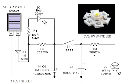
This portable solar lantern circuit uses 6 volt/5 watt solar panels are now widely available. With the help of such a photo-voltaic panel we can construct an economical, simple but efficient and truly portable solar lantern unit. Next important component required is a high power (1watt) white LED module.

When solar panel is well exposed to sunlight, about 9 volt dc available from the panel can be used to recharge a 4.8 volt /600 mAh rated Ni-Cd batterypack. Here red LED (D2) functions as a charging process indicator with the help of resistor R1. Resistor R2 regulates the charging current flow to near 150mA.

Solar Lantern Circuit Schematic
Circuit Project: Portable Solar Lantern

Assuming a 4-5 hour sunlit day, the solar panel (150mA current set by the charge controller resistor R2) will pump about 600 – 750 mAh into the battery pack. When power switch S1 is turned on, dc supply from the Ni-Cd battery pack is extended to the white LED (D3). Resistor R3 determines the LED current. Capacitor C1 works as a buffer.

Note: After construction, slightly change the values of R1,R2 and R3 up/down by trial&error method, if necessary.


Source by :http://www.extremecircuits.net/2012/08/portable-solar-lantern.html
Read More..

Thursday, September 18, 2014

Portable Muscular Bio Stimulator

This is a small, portable set, designed for those aiming at look improvement. The Bio-Stimulator provides muscles stimulation and invigoration but, mainly, it could be an aid in removing cellulite. Tape the electrodes to the skin at both ends of the chosen muscle and rotate P1 knob slowly until a light itch sensation is perceived. Each session should last about 30 - 40 minutes. 

Circuit diagram :
Portable Muscular Bio-Stimulator-Circuit Diagram
Portable Muscular Bio-Stimulator Circuit Diagram

C1 generates 150µSec. pulses at about 80Hz frequency. Q1 acts as a buffer and Q2 inverts the polarity of the pulses and drives the Transformer. The amplitude of the output pulses is set by P1 and approximately displayed by the brightness of LED D1. D2 protects Q2 against high voltage peaks generated by T1 inductance during switching.
Parts :
  • P1-----4K7 Linear Potentiometer
  • R1-----180K   1/4W Resistor
  • R2-----1K8  1/4W Resistor (see Notes)
  • R3-----2K2  1/4W Resistor
  • R4-----100R   1/4W Resistor
  • C1-----100nF  63V Polyester Capacitor
  • C2-----100µF  25V Electrolytic Capacitor
  • D1-----LED  Red 5mm.
  • D2-----1N4007  1000V 1A Diode
  • Q1,Q2-----BC327  45V 800mA PNP Transistors
  • IC1-----7555 or TS555CN CMos Timer IC
  • T1-----220V Primary, 12V Secondary 1.2VA Mains transformer (see Notes)
  • SW1-----SPST Switch (Ganged with P1)
  • B1-----3V Battery (two 1.5V AA or AAA cells in series etc.)
Notes :
  • T1 is a small mains transformer 220 to 12V @ 100 or 150mA. It must be reverse connected i.e. the 12V secondary winding across Q2 Collector and negative ground, and the 220V primary winding to output electrodes.
  • Output voltage is about 60V positive and 150V negative but output current is so small that there is no electric-shock danger.
  • In any case P1 should be operated by the "patient", starting with the knob fully counter-clockwise, then rotating it slowly clockwise until the LED starts to illuminate. Stop rotating the knob when a light itch sensation is perceived.
    Best knob position is usually near the center of its range.
  • In some cases a greater pulse duration can be more effective in cellulite treatment. Try changing R2 to 5K6 or 10K maximum: stronger pulses will be easily perceived and the LED will shine more brightly.
  • Electrodes can be obtained by small metal plates connected to the output of the circuit via usual electric wire and can be taped to the skin. In some cases, moistening them with little water has proven useful.
  • SW1 should be ganged to P1 to avoid abrupt voltage peaks on the "patients" body at switch-on, but a stand alone SPST switch will work quite well, provided you remember to set P1 knob fully counter-clockwise at switch-on.
  • Current drawing of this circuit is about 1mA @ 3V DC.
  • Some commercial sets have four, six or eight output electrodes. To obtain this you can retain the part of the circuit comprising IC1, R1, R2, C1, C2, SW1 and B1. Other parts in the diagram (i.e. P1, R3, R4, D1, D2, Q2 & T1) can be doubled, trebled or quadrupled. Added potentiometers and R3 series resistors must be wired in parallel and all connected across Emitter of Q1 and positive supply.
  • Commercial sets have frequently a built-in 30 minutes timer. For this purpose you can use the Timed Beeper the Bedside Lamp Timer or the Jogging Timer circuits available on this Website, adjusting the timing components to suit your needs.
Disclaimer: we cant claim or prove any therapeutic effectiveness for this device.

Source :www.ecircuitslab.com
Read More..

Thursday, September 11, 2014

Build a Portable Nicad Battery Charger Wiring diagram Schematic

This is a Portable Nicad Battery Charger Circuit Diagram. This schema can you build easily, The portable charger is intended primarily to give model enthusiasts the opportunity of charging their Nicad batteries from a car battery out in the open. The supply voltage for the schema is regulated by IC1. When the schema is connected to the car battery, D2 lights only if the Nicad to be charged has been connected with correct polarity. For that purpose, the + terminal of the Nicad battery is connected to the base of T1 via R8. Because even a discharged battery provides some voltage, T1 is switched on and D2 lights. 

 Portable Nicad Battery Charger Circuit Diagram


Portable

Only if the polarity is correct will the pressing of the start switch, SI, have any effect. If so, the collector voltage of T1 is virtually zero so that monostable IC2 is triggered by SI. The output, pin 3, of this CMOS timer then becomes high, T2 is switched on and relay Rel is energized. Charging of the Nicad battery, via R5 and D6, then begins and charging indicator D4 lights. During the charging, C4 is charged slowly via PI and R4. The value of these components determines the mono time of IC2 and thus the charging period of the Nicad battery. With values as shown in the diagram, that period can be set with PI to between 26 and 33 min. Notice that this time is affected by the leakage current of C4; use a good-quality capacitor here. 

The charging can be interrupted with reset switch S2. The charging current through the Nicad battery is determined by the value of R, which can be calculated: Ic is the charging current, which is here because the chosen charging period is twice the nominal value of the capacity of the Nicad battery. Resistor R must be able to dissipate a power of 1/ R W. Finally, make sure that the Nicad battery is suitable for fast charging; never charge for longer than half an hour! 
Read More..