Showing posts with label for. Show all posts

Monday, October 27, 2014

Most Power Supply for Amplifier

As with most power amplifiers, the ±60 V power supply need not be regulated. Owing to the relatively high power output, the supply needs a fairly large mains transformer and corresponding smoothing capacitors—see circuit diagram below.

Note that the supply shown is for a mono amplifier; a stereo outfit needs two supplies. 

The power supply is straightforward, but can handle a large current. Voltage acserves as drive for the power-on delay circuit. The transformer is a 625 VA type, and the smoothing capacitors are 10 000 µF, 100 V electrolytic types. The bridge rectifier needs to be mounted on a suitable heat sink or be mounted directly on the bottom cover of the metal enclosure.. The transformer needs two secondary windings, providing 42.5 V each. The prototype used a toroidal transformer with 2x40 V secondaries. The secondary winding of this type of transformer is easily extended: in the prototype 4 turns were added and this gave secondaries of 2x42.5 V.
Read More..

Sunday, October 26, 2014

Antenna Input Audio Lineout Adaptor For Portable Radios

Here is an idea for a simple low-cost adaptor that allows a portable FM radio (or MP3 player with FM tuner) to be connected to an external antenna and to audio equipment such as a hifi system or PC sound card. Portable FM radios and some MP3 players typically provide a 3.5mm stereo jack socket for the headphone connection, with the shield conductor of the headphone cable doubling as an antenna.

The problem:

Recently, the author bought a cheap FM radio with a USB connector, designed to be operated with a PC. The package included an audio cable with a 3.5mm stereo phone plug at each end. The plug that goes into the radio has an additional wire (about 2m long) hanging out of it, which is meant to serve as an indoor antenna. When using the supplied cable, the system suffered from poor radio reception (too much interference), and poor audio quality (lack of bass). The first problem was easily explained, as the radio was used in a marginal TV/FM reception area. When the cable was "buzzed out", the reason for the second problem became apparent.

There was no audio ground connection, as the cable screen is not connected to anything at the radio end! As mentioned, the antenna wire in these units is connected to the "common" terminal of the 3.5mm socket, which normally doubles as the audio signal return path. If this terminal were to be connected to the ground of external audio equipment, the antenna signal would be clobbered. Perhaps the designer of this cable assumed that an adequate audio ground connection would be made indirectly via the USB cable – a poor assumption!

Circuit diagram:
The challenge:

The challenge then was to provide a good antenna signal for the radio while at the same time making a good audio ground connection to external equipment. Preferably, this was to be achieved without relying on the USB connector (because not all FM radios have one) and without having to mess with the radio’s internal works. The accompanying circuit diagram shows how this can be achieved. The radio-frequency choke (L1) has a low impedance at audio frequencies, thereby making an audio ground path to the line output sockets from the radio’s antenna input ("common" terminal).

Conversely, the RFC presents a high impedance to the RF antenna signal, so preventing it from being shorted to ground. The antenna signal is coupled to the radio via two 220pF polystyrene (or ceramic) capacitors, which also block low-frequency interference (eg, mains hum). Note that the design relies on the capacitance in the audio cable to couple the antenna "ground" (cable shield) to the radio’s internal "ground".

Building it:

To build the adaptor, simply mount the parts in a small plastic box and wire up as shown. A suitable choke is available from Jaycar (Cat. No. LF-1534). The leads going to the 3.5mm plug should be no longer than about 100mm and need not be shielded. With a good TV/FM antenna, the author’s unit performed remarkably well, even in a poor FM reception area. The audio frequency response and signal-to-noise ratio were surprisingly good considering the low cost of the radio (about $40).
Author: Michael Bauer - Copyright: Silicon Chip Electronics
Read More..

Saturday, October 25, 2014

Simple Indicator for Dynamic Limiter Schematic Diagram

The indicator described here is specifically designed for adjusting the dynamic limiter described elsewhere in this edition and checking whether the maximum level of the reference voltage (P1) needs to be modified. Her e we use a 4 -to -16 decoder IC (type 4514) to monitor the state of the four-bit up/down counter in the limiter circuit. This IC can be powered from the ±8 V supply voltages of the limiter. The limiter board has a 6-way connector (K5) that provides access to the four counter outputs and the sup-ply voltages. Connector K1 of the indicator circuit can be connected to K5 on the limiter board.
 Indicator for Dynamic Limiter Schematic

One output of the 4514 goes high for each unique 4-bit combination on its inputs, while the other outputs remain logic Low. A separate current-limiting resistor is connected in series with each LED. It was not possible to use a common cathode resistor here because most LEDs have a maximum reverse blocking voltage of only 5 V, while the supply voltage here (16 V) is a good deal higher.

The 16 LEDs ar ranged in a r ow pr ov ide a ‘fluid’ indication of the control process. You can enhance the display by using different colours for the first and last LEDs, such as red for D1 (maximum gain) and green for D16 (minimum gain), with yellow for the rest of the LEDs. While observing signals from various sources (TV set, DVD, media player, etc.), you can easily use the 16 LEDS to monitor the behaviour of the limiter and adjust the setting of potentiometer P1 in the limiter circuit. It must be set such that D16 only lights up at the maximum signal level. If this is not possible and D16 remains lit a good deal of the time regardless of the position of P1, it will be necessar y to increase the value of P1. Of course, it is also poss-ible to adjust P1 so the strongest signal source extends slightly above the control range of the limiter.

This circuit can easily be assembled on a small piece of prototyping board. The current consumption is around 4 mA. link
Read More..

Universal Tester for 3 pin Devices

Most 3-terminal active components can be  tested statically using just an ohmmeter. But  when you have a lot of these devices to test,  the procedure soon becomes boring. That’s  where the idea came from to combine fast,  easy testing for these types of device into a  single instrument. 

The unit described here enables you to test  NPN and PNP bipolar transistors, N-or Pchannel FETs or MOSFETs, UJTs, triacs, and thyristors. Regardless of the type of device, the  tests are non-destructive. Universal connectors allow testing of all package types, including SMDs (up to a point). The unit lets you  change from one type of device to another in  a trice. It avoids using a multi-pole switch, as  they’re too expensive and hard to find. 
.
Circuit diagram :
Universal Tester for 3-pin Devices-Circuit Diagram
Universal Tester for 3-pin Devices Circuit Diagram
.
Here’s how to build a versatile instrument at  a ridiculously low cost. IC1 is a 4066 quad CMOS switch which will let us switch between bipolar transistors and FETs. LEDs D1–D4 tell us about the condition  of the test device, when we press the ‘Test’  button. The 4066 can only handle a few milliamps, not  enough for the other component types to be  tested, hence the reason for using relay RE1.  This 12 V relay offers two NO contacts. The  first applies power to the UJT test circuit, the  second applies it to the triac and thyristor test  circuit. 
.
Extensive testing has shown that the best way  to test UJT transistors is to do so dynamically,  with the help of a relaxation oscillator. Net-work R11/C1 sets the oscillator frequency to  around 2 Hz. On pin B1 of the UJT we find a  nice sawtooth, which is not of much interest  to us here. However, pin B2 gives good but  very short pulses. IC2, wired as a monostable,  lengthens these pulses so they can be clearly  seen via LED D5. 

The relay’s second pole is going to drive the  thyristor’ sortriac’s trigger pin. The value of  R18 is a good compromise with respect to the varying trigger currents for this type of  device. Resistor R17 is important, as the hold-ing current must be high enough for a triac;  250 mA is a good compromise. LED D6 tells  you if the device is in good condition or not;  but watch out, the test result must be con-firmed by briefly cutting the power in order  to reset the triac. 

On the web page for this article [1] you’ll find  the author’s CAD files (PCB layout and front  panel) along with some photos of his project.  On the prototype, the LEDs and the ‘Test’  button were wired onto the copper side of  the PCB. The six female connectors for the  devices being tested were salvaged, but there  are lots of models available on the market (the  pitch is standard). The test cable crocodile  clips must be as small as possible for testing  SMD devices.
Read More..

Friday, October 24, 2014

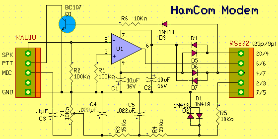
Modem for Digital Modes Circuits Diagram

Ham Com is a modem for almost all types of digital transmission for radio amateurs. It can be used to RTTY, ASCII, NevTex, Sitor, Amtor, Fec, CW, FSK, etc.. The modem is simple and can even be used for receiving faxes and SSTV wx-using JV-FAX software.

 Modem for Digital Modes Circuits Diagram

Modem for Digital Modes Circuits Diagram


To use this modem, you need a PC with serial port, Software HamCom and radio equipment.
Read More..

Monday, October 20, 2014

Three Flashing LED Doorbells For The Hearing Impaired

When the push switch is operated - the buzzer will sound and the LEDs will begin to flash. For the hearing members of the household - the buzzer acts as a regular doorbell. It also re-assures the visitor that the doorbell is working.

When the push switch is released the buzzer will stop - but the LEDs will continue to flash. The length of time they will go on flashing is set by the values of R2 & C1. With the values shown in the diagram - the LEDs will flash for a further 30 seconds or so. If you make R2 a variable resistor, you can adjust the time period. If you want longer than 30 seconds - increase the value of C1 or R2.

Flashing-LED-Doorbells-Circuit-Diagram

The last circuit will flash up to two groups of 3 LEDs in tandem. This circuit will flash the two groups alternately. The alternate flashing creates the illusion of movement - and makes the display more eye-catching. Note that - although Ive drawn the two groups of LEDs side by side - the individual LEDs can be mounted in any pattern you like.

LED-Doorbells-Circuit-Diagram
The main difference between this circuit and the last one - is the addition of the two transistor switches. The switches will each flash up to 15 groups of 3 LEDs. And - because they are getting power directly from the battery - the LEDs will glow at their full brilliance.
Three-Flashing LED-Doorbells-Circuit-Diagram
The Support Material for these circuits includes detailed circuit descriptions - and all the information you need to adapt them to a different supply voltage. link
Read More..

Fan Speed ​​Control for Temperature Circuit Diagram

With this simple circuit that you will be able to control the speed of a DC fan according to the temperature measured by a temperature sensor. It is an ideal accessory for your projects that require cooling that are not constant. 

This simple design allows precise speed control of motors, fans, and blowers, proportional to the temperature. An NTC thermistor (R1) is used as temperature sensor. A circuit optional was added to remotely monitor the operation of the fan and to allow some kind of indication of the approximate speed by increasing the brightness of an LED.

 Fan Speed ​​Control for Temperature Circuit Diagram

 Fan Speed ​​Control for Temperature Circuit Diagram


The R5 must be configured to allow the engine just starting to run at the desired temperature. Any 6K8 between the NTC thermistor 22K can operate provided that the R2 value is one tenth of the thermistor. R6, R7 and D1 are optional: R7 obligation is adjusted until the LED glow dimly when the engine is just running.

Parts List
R1 15K @ 20 ° C NTC Thermistor (See Notes)
R2 1K5 1/4W Resistor (See Notes)
R3 1K 1/4W Resistor
R4 270R 1/4W Resistor 1/2W
R5 22K Trimpots
R6 680R 1/4W Resistor (Optional, see Notes)
R7 470R Trimpots
C1 100μF 25V Electrolytic Capacitor
LED D1 (Optional, any shape and color, see Notes)
Q1 BC547 45V 100mA NPN Transistor
Q2 BD140 80V 1.5A PNP Transistor
M1 Fan Motor 12V 700mA max.
Read More..

Saturday, October 18, 2014

MJ2955 for IC 78xx Boosting Regulator Current Diagram Circuit


Source :: http://www.zen22142.zen.co.uk/Circuits/Power/boosti.htm

IC 78xx series of voltage regulators are available with different current outputs, you can boost the available current output with this circuit. A power transistor is used to supply extra current to the load the regulator, maintaining a constant voltage. Currents up to 650mA will flow through the regulator, above this value and the power transistor will start to conduct, supplying the extra current to the load. This should be on an adequate heat sink as it is likely to get rather hot. Suppose you use a 12v regulator, 7812. The input voltage should be a few volts higher to allow for voltage drops. Assume 20 volts. Lets also assume that the load will draw 5amps. The power dissipation in the transistor will be Vce * Ic or (20-12)*8=40watt. It may keep you warm in the Winter, but you will need a large heatsink with good thermal dissipation. If you want to Boost the output current with a negative regulator, such as the 79xx series, then the circuit is similar, but an NPN type power transistor is used instead.
Read More..

Friday, October 17, 2014

Extend Timer Range For The 555 Circuit Diagram

Anyone who has designed circuits using the 555 timer chip will, at some time have wished that it could be programmed for longer timing periods. Timing periods greater than a few minutes are difficult to achieve because component leakage currents in large timing capacitors become significant. There is however no reason to opt for a purely digital solution just yet. The circuit shown here uses a 555 timer in the design but nevertheless achieves a timing interval of up to an hour! The trick here is to feed the timing capacitor not with a constant voltage but with a pulsed dc voltage. The pulses are derived from the un smoothed low voltage output of the power supply bridge rectifier.

Extend Timer Range For The 555 Circuit Diagram


The power supply output is not referenced to earth potential and the pulsing full wave rectified signal is fed to the base of T1 via resistor R1. A 100-Hz square wave signal is produced on the collector of T1 as the transistor switches. The positive half of this waveform charges up the timing capacitor C1 via D2 and P1. Diode D2 prevents the charge on C1 from discharging through T1 when the square wave signal goes low. Push-button S1 is used to start the timing period. This method of charging uses relatively low component values for P1 (2.2 MΩ) and C1 (100 to 200 µF) but achieves timing periods of up to an hour which is much longer than a standard 555 circuit configuration.
Read More..

Thursday, October 16, 2014

Simple Knight Rider lights Circuit for model cars

This simple circuit drives 6 LEDs in Knight Rider scanner mode. Power consumption depends mainly on the type of LEDs used if you use a 7555 (555 CMOS version).


Simple Knight Rider lights Circuit

Simple


Note
That VDD and GND for the ICs are not shown in the circuit drawing.

Pin-outs:
(7)555 4017
1 GND 1 Q5 9 Q8
2 TRIGGER 2 Q1 10 Q4
3 OUTPUT 3 Q0 11 Q9
4 RESET 4 Q2 12 CO
5 CONTROL VOLTAGE 5 Q6 13 NOT ENABLE
6 THRESHOLD 6 Q7 14 CLK
7 DISCHARGE 7 Q3 15 RESET
8 VDD 8 GND 16 VDD
Read More..

Wednesday, October 15, 2014

Audio Power Amplifier for AM Radio Circuit Diagram

This is an AM radio power amplifier circuit. What is different with other general amplifier is that this circuit has a low-pass filter (passive type), built using R1C1 to limit the input-output frequency response. Additionally, a ferroxcube K5-001-001/3B with 3 turns of wire is used as ferrite bead  at output filter. All components should be spaced very close to  the IC. 

The ground and speaker lead must be twisted tightly. The supply lead and supply ground also must be twisted very tightly. Here is the schematic diagram of the  circuit.

 Audio Power Amplifier for AM Radio Circuit Diagram

Audio

Read More..

Best Start up Aid for PCs

Since one of the servers owned by the author would not start up by itself after a power failure this little circuit was designed to perform that task. 

The older PC that concerned did have a standby state, but no matching BIOS set-ting that allows it to start up unattended. Although a +5 V standby supply voltage is available, you always have to push a but-ton for a short time to start the computer up again. Modern PCs often do have the option in the BIOS which makes an automatic start after a power outage possible. After building in the accompanying circuit, the PC starts after about a second. Incidentally, the push-button still functions as before.
 

The circuit is built around two golden oldies: a NE555 as single-shot pulse generator and a TL7705 reset generator. The reset generator will generate a pulse of about 1 second after the supply voltage appears. The RC circuit between the TL7705 and the NE555 provides a small trigger pulse during the falling edge of the 1 second pulse. The NE555 reacts to this by generating a nice pulse of 1.1RC. During that time the output transistor bridges the above mentioned pushbutton switch of the PC, so it will start obediently. 

Pcs
Other applications that require a short duration contact after the power supply returns are of course also possible.

 
Author : Egbert Jan van den Bussche – Copyright : Elektor
Read More..

Monday, October 13, 2014

Signal Amplifier For TV explanation Charecteristics and circuit

 This is a small, broad band, signal amplifier which covers the frequencies from 40 to 900 MHz. These frequencies include TV in VHF and UHF and also the radio broadcasting frequencies in the 88 - 108 MHz FM band.
It is connected between the antenna and the input of your receiver and boosts the signals by up to 20 dB, thus making it possible to receive even the weakest signals.

Pcb.gif
Dimensions (4,3cm x 5,4cm)
Technical Specifications -Characteristics

Frequency response: 40 - 900 MHz
Gain: . 20 dB
Maximum output level: 90 uV
Input - output impedance: 75 ohm
How it Works

The circuit is built around a single transistor a UHF low signal device, the BFW 92. This transistor can operate in frequencies as high as 1.6 GHz, and has a gain of 23 dB. The signal from the antenna is applied to the input of the circuit and through C5 is fed to the base of the transistor. It is amplified and from the collector of the BFW 92 through C2 and C1 is taken to the input of the radio or TV receiver.
The circuit operates off a small 9 V battery which, because of the very low power consumption of the circuit, is going to last for a very long time.


Circuits


Construction

First of all let us consider a few basics in building electronic circuits on a printed circuit board. The board is made of a thin insulating material clad with a thin layer of conductive copper that is shaped in such a way as to form the necessary conductors between the various components of the circuit. The use of a properly designed printed circuit board is very desirable as it speeds construction up considerably and reduces the possibility of making errors. Smart Kit boards also come pre-drilled and with the outline of the components and their identification printed on the component side to make construction easier. To protect the board during storage from oxidation and assure it gets to you in perfect condition the copper is tinned during manufacturing and covered with a special varnish that protects it from getting oxidised and also makes soldering easier.
Soldering the components to the board is the only way to build your circuit and from the way you do it depends greatly your success or failure. This work is not very difficult and if you stick to a few rules you should have no problems. The soldering iron that you use must be light and its power should not exceed the 25 Watts. The tip should be fine and must be kept clean at all times. For this purpose come very handy specially made sponges that are kept wet and from time to time you can wipe the hot tip on them to remove all the residues that tend to accumulate on it. DO NOT file or sandpaper a dirty or worn out tip. If the tip cannot be cleaned, replace it. There are many different types of solder in the market and you should choose a good quality one that contains the necessary flux in its core, to assure a perfect joint every
time.
DO NOT use soldering flux apart from that which is already included in your solder. Too much flux can cause many problems and is one of the main causes of circuit malfunction. If nevertheless you have to use extra flux, as it is the case when you have to tin copper wires, clean it very thoroughly after you finish your work. In order to solder a component correctly you should do the following:
- Clean the component leads with a small piece of emery paper.
- Bend them at the correct distance from the component’s body and insert the component in its place on the board.
- You may find sometimes a component with heavier gauge leads than usual, that are too thick to enter in the holes of the p.c. board. In this case use a mini drill to enlarge the holes slightly. Do not make the holes too large as this is going to make soldering difficult afterwards.
- Take the hot iron and place its tip on the component lead while holding the end of the solder wire at the point where the lead emerges from the board. The iron tip must touch the lead slightly above the p.c. board.
- When the solder starts to melt and flow, wait till it covers evenly the area around the hole and the flux boils and gets out from underneath the solder. The whole operation should not take more than 5 seconds. Remove the iron and leave the solder to cool naturally without blowing on it or moving the component. If everything was done properly the surface of the joint must have a bright metallic finish and its edges should be smoothly ended on the component lead and the board track. If the solder looks dull, cracked, or has the shape of a blob then you have made a dry joint and you should remove the solder (with a pump, or a solder wick) and redo it.
- Take care not to overheat the tracks as it is very easy to lift them from the board and break them.
- When you are soldering a sensitive component it is good practice to hold the lead from the component side of the board with a pair
of long-nose pliers to divert any heat that could possibly damage the component.
- Make sure that you do not use more solder than it is necessary as you are running the risk of short-circuiting adjacent tracks on the board, especially if they are very close together.
- When you finish your work, cut off the excess of the component leads and clean the board thoroughly with a suitable solvent to
remove all flux residues that may still remain on it.

The project is a very easy one, as the components which form the circuit are very few and their outlines have been clearly stencilled on the board for you. The only unusual thing is that the transistor must be soldered from the copper side of the board. This is, however, common with UHF devices and is usually done to avoid the introduction of stray capacitances between the transistor’s leads that could possibly alter the behaviour of the circuit. Be careful to make good joints and try to keep the component leads as short as possible because of the very high frequencies involved. Solder first of all the pins and the resistors. The coils are supplied ready to be soldered on the printed circuit and you
should take care not to deform them in the process. Place then the capacitors and solder the diodes carefully trying to avoid overheating them and making sure that they are correctly aligned. Solder the transistor in its place, after you have finished soldering the other components, to avoid overheating it, and be careful to align it according to the diagram included in the instructions. (The lettering on the transistor body should be facing away from the copper). The input of the circuit is at point 4 and ground and the output at point 1 and ground. The battery is connected using the battery clip supplied at points 2 (-) and 3 (+), and is a miniature 9 V one, alkaline if you prefer. For best performance and to avoid unwanted interference during operation it is recommended to place the circuit in a small metal box, and use suitable connectors mounted on the box for the external connections. You can use a box large enough to house the amplifier and the battery or you can use an external power supply, but remember to use a FEED THROUGH capacitor on the positive supply line, where it passes through the metal box. If you plan to use the amplifier for both VHF and UHF TV reception you should use a common VHF/UHF mixer before the amplifier’s input.
PARTS
R1 = 120 Ohm (brown, red, brown)
R2 = 1,5 KOhm (brown, green, red)
R3 = 270 Ohm (red, violet, brown)
R4 = 82 KOhm (gray, red, orange)
C1,C5 = 100pF (ceramic)
C2,C3 = 1nF (ceramic)
C4 = 2,2pF (ceramic)
D1,D2 = 1N4148 diode
Transistor = BFR90, BFR91, BFW92
Misc = PCB, 6pins, solder, 9V battery clip
Read More..

Sunday, October 5, 2014

A Simple Crossover Circuit for Tweeter

A single coil speaker is not good in handling high and low frequency at the same time. If we could filter out the low frequency and play it through a tweeter, it will produce more sound quality than using a single speaker. In this figure shows the answer for the problem in above. This is a simple design circuit for protected thee voltage and current in tweeter speaker.


The concept of operation this circuit is the speaker that can protected is tweeter with 4 or 8 ohm impedance. R1 is a potentiometer resistor that used to adjust matching the tweeter speaker output level to that of woofer. R1 should be rated more than 2 Watts.
Read More..

Friday, September 19, 2014

Pulse Charger for Reviving Tired Lead Acid Batteries

If you own a motorcycle, a motor home, a caravan, a lawn mover, a day cruiser or maybe a vintage car you must at some point had to write off a lead acid battery. When a battery is improperly charged or allowed to self-discharge as occurs during non-use, sulphate crystals build up on the batterys plates. The sulphate preventing the battery from being fully charged and therefore it is unable to deliver its full capacity. When trying to charge a battery in this state it only gets hot and looses water, the gravity of the electrolyte is not increasing to its normal “full charge” state. The only thing you do is killing the battery completely. If a battery has a resting voltage of at least 1.8 Volts/cell and no cells are shorted, desulphation of its plates can be done. This circuit is an add-on and part for a modification of a normal charger and it takes care of the sulphate problem. Pulse Charger for Reviving Tired Lead Acid Batteries Circuit diagram: CAUTION: Before you begin a project like this remember: mains voltage is dangerous so if you are not 100% sure of what you’re doing consult a friend who has the skills or, don’t do it at all ! The project: get hold of an old charger, big or small it’s your choice depending on the size of batteries you normally handle (bigger is better). There are some tricks to boost the performance if you need it. Start by ripping out everything except the transformer and the rectifier. Some older chargers are equipped with fin rectifiers, which have high voltage drop and must be replaced. Replace with a rugged bridge rectifier that can cope with the amperes. All wiring on secondary should be short and heavy wire. The rectifier should be bolted to the chassis to keep cool. If the charger have a high/low switch it’s a bonus, if not you can in some cases add a few turns of wire on the secondary winding. The circuit; a 14-stage ripple counter and oscillator IC 4060 produce a pulse, which is the heartbeat of the circuit. The pulse is feed to the 555 timer that deicide the length of the active output. With the switch you can select long or short pulse output. The output of the 555 timer triggers the zero-cross optoisolator triac driver MOC 3041 via a transistor. This gives the charger transformer a soft start via the triac and the snubber circuit. A small power supply is necessary for the circuit and consists of T1 a transformer 15V 0.1A secondary, a bridge rectifier, a regulator and two caps. Because this project include a charger that is (X) the outcome can differ in performance from one case to another. However this do not mean that your project doesn’t work, but the efficiency can vary. Some notes the snubbercap is a high voltage AC type (X) and the resistors on the mains side is at least 0.5W type. Use a triac that can take 400V+ and 10A+, I use BTA 25.600 but this is overkill in most cases. No PCB sorry! How it works: Well the short version. The object is to get the cell voltage high enough for the sulphate to dissolve without boiling or melting the battery. This is achieved by applying higher voltage for shorter periods and let the battery rest for a while. The pulses on short range is about 0.5s on / 3s off and the long pulse range is 1.4s on / 2s off. These times can vary depending on component tolerances. Start on long pulse and if you discover “boiling” (more than with normal charging) in the electrolyte switch to short puls. Don’t leave the process unattended, at least until you know how your specific version of this project turns out. I built ver.1 of this circuit some 10 years ago and have experimented with it but I’m sure someone can improve it further.

Good Luck! Ante
Ante135@hotmail.com

Read More..

Monday, September 15, 2014

Control Switch for Fan and Air Conditioner

An electronic switch that can be used to switch on both the air-conditioner as well as fan of your room, one by one. The schema consists of power supply and control sections. The power supply section is built around transformer X1, bridge rectifier BR1 and filter capacitor C1. The 50Hz, 230V AC mains is stepped down by transformer X1 to deliver a secondary output of 9V, 300 mA. The transformer output is rectified by the bridge rectifier and filtered by capacitor C1.

Control Switch for Fan and Air-Conditioner  Circuit Diagram


When the mains is switched on for the first time, pin 3 of IC CD4017 (IC1) goes high and relay RL1 energies to switch on the fan. When mains is briefly switched off using S1 and then switched on, the power to IC1 is maintained by the charge on capacitor C1. At the same time, there is a trigger pulse on the clock input (pin 14) of IC1, which advances the decade counter and relay RL2 energies to switch-on the air-conditioner. Both the air-conditioner and the fan will be turned off if the switch is in the ‘off’ position.

Assemble the schema on a general-purpose PCB and enclose in a suitable case. Fix the unit onto the switchboard. Use relays RL1 and RL2 with proper contact ratings. The current rating depends on the load that you are going to control.
Read More..

Thursday, September 11, 2014

How to create a simple adjusting volume for amplifier

This circuit usually used for amplifier that do not require additional device in one box amplifiers. Enhancements such as Equalizer , Tone Control , Mixer , etc.  Only by requiring a potentiometer mono or stereo if stereo power amplifier , and few  cables you can make this circuit easily.
See picture below :

 
 First connect the cable from the power amplifier input to pin2 potentio , and connect ground to pin 1 , then connect the output of tuner or other media player to pin 3. Try turning to the right then the sound will be high , and if played left back then the sound will below.
Read More..

Wednesday, September 10, 2014

Cheap Electronics Component for Amplifier Application

cheap
Cheap electronics component for amplifier application, it is simple to be made for speaker active . The sound quality even this  Mini Amplifier TDA2030 quite satisfactory for a portable audio system.
Read more
Read More..

Saturday, September 6, 2014

Batteries Charger PSU Ideal for Digital Cameras

This schema was created for digital cameras. Its known the digital cameras have considerable power consumption. For example my camera Minolta E223 requires approximately 800 mA. In practice a mains power supply or high capacity NiMH accumulators (batteries) can satisfy this demand. Batteries Charger & PSU Circuit diagram: This schema consists of two parts, charger and adapter. The transformer, rectifier bridge and buffer condensator are common. Adapter is quite simply its main part is an adjustable voltage regulator LM 317 according to usual setting. Output is a suitable for camera jack plug. Voltage can be adjusted in range 2-9 V. In the charger schema a 7805 fixed voltage regulator works as current generator assured constant current during charging. This charging current can be adjusted with the 100 /1W potentiometer in range about 50-300 mA indicated by a small current measuring instrument. From one to four batteries can be charged simultaneously. The switch must be set according to number of batteries, and charging current of batteries given by manufacturer must be adjusted. This schema doesnt measure charging time and charging condition of batteries. Manufacturers give charging time, usually 14-16 h. I solved this problem with a simply, cheap mechanical mains timer. I think its accuracy is sufficient.  

Sandor Dobany from Hungary
dsandor@minimail.hu

Read More..

Simple Comparator for Over Voltages Wiring diagram Schematic

This is the Simple Comparator for Over Voltages Circuit Diagram. Comparator is a device that compares two voltages or currents and outputs a digital signal indicating which is larger. It has two analog input terminals V_+, and V_-, and one binary digital output V_o,. The output is ideally. To maintain an alarm condition when an overvoltage transient disappears, add an SCR to the comparator diagram. For SCR operation, voltages to the comparator inputs are inverted. (B) The triple-voltage monitoring schema detects transient power-supply over-voltages.If excessive voltage momentarily appears at the 5, 12 and -12 V inputs, the LED for that schema lights and the beeper sounds for as long as the .

Simple Comparator for Over Voltages Circuit Diagram

Simple

Read More..